Project 05 of 11: 项目 05 / 11:GaN Quadrotor ESC Final-Year ProjectGaN 四旋翼电调毕业设计
For my XJTLU final-year project I built a quadrotor ESC around INN100EA035A GaN FETs and LMG1210 drivers, with a Si MOSFET board as the reference. After five board spins, one spectacular shoot-through and an AM32 port, both boards finished a propeller-loaded comparison at matched speeds of 3000, 6500 and 10000 rpm.西浦本科毕设。我用 INN100EA035A 氮化镓功率管和 LMG1210 驱动做了一块四旋翼电调,再做一块 Si MOSFET 电调作参考。打了五次板,炸过一次很壮观的直通,移植了 AM32,最后两块板在 3000、6500、10000 rpm 三个对齐的转速下完成了带桨对比。
Topic and GaN Route选题与 GaN 路线
The first thing I searched the school's final-year topic list for was flight controllers. Nobody on it worked on them. Drone hardware was what I was after: a sensorless FOC side project had already got me hooked on motor drives, Bilibili kept serving me drone-build videos, and I had my eye on DJI. In the second half of 2025 DJI sat unchallenged at the top of the drone industry, and the people who had worked there all told roughly the same story: brutal hours, top-of-market pay, and you learn real things fast. A project as close to drone hardware as I could get was the obvious move.
学院发下来的毕设题目列表,我第一个搜的是飞控,结果一个做飞控的老师都没有。想做无人机硬件,原因很实在:那阵子正折腾无感 FOC,对电驱本来就上头,B 站又天天给我推组装无人机的视频,更重要的是想去大疆。2025 年下半年,大疆在无人机行业是纯纯的龙头,从里面出来的人讲经历,几乎清一色都说累、薪资行业顶尖、能飞快学到真东西。毕设当然要找一个和无人机硬件贴得越近越好的。
Without a flight controller, the next best thing was the motor controller underneath it. Prof. Tianru Zhang, whose research covers motor drives and power electronics, was offering a quadrotor electronic speed controller, and I got the place after the interview. Cheap modular ESCs are everywhere, though, and building yet another one felt pointless. Through 2025 GaN was the power device everyone suddenly cared about, turning up in phone chargers and EV drive platforms alike, so why not in a drone ESC? I put the idea to Prof. Zhang. "Sure, go for it," he said, and that was the project.
飞控没有,退一步就是电调。张天如老师正好有一个四轴无人机电调的题目,他的方向是电驱和电力电子,面试过了就定了下来。可网上现成的模块化小电调到处都是,照着再做一块意思不大,总得做点不一样的。2025 年一整年,氮化镓在功率器件里非常出圈,手机充电器在用,汽车电驱平台也在用,那它能不能用在无人机电调上?跟老师一说,老师说可以啊,没问题,你做吧。
Two ESC Boards两块电调板
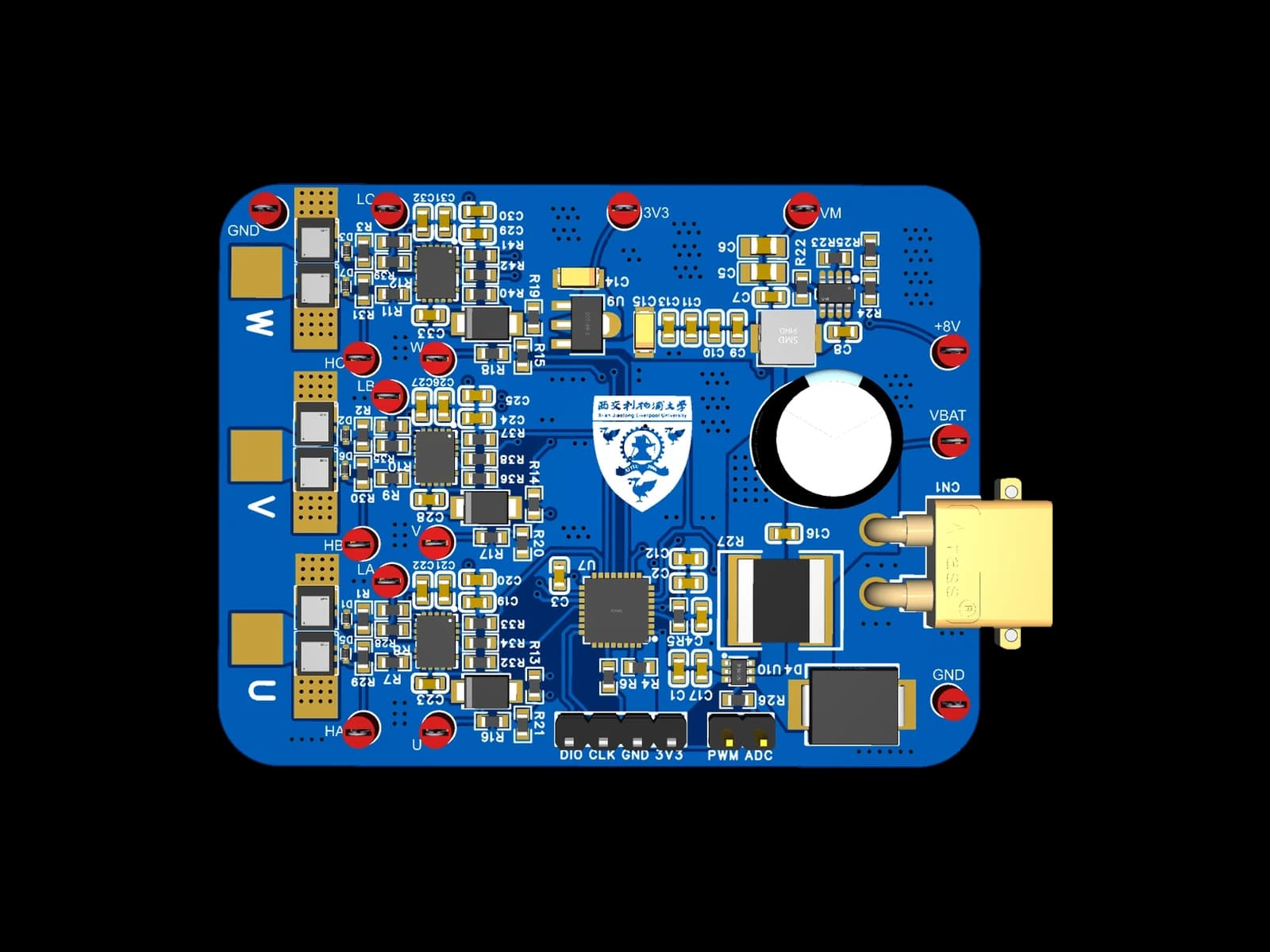
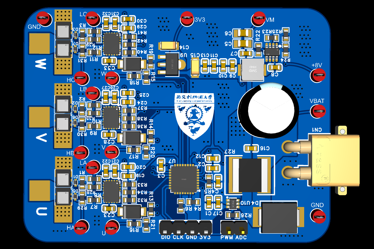
I pitched the work as two parallel routes and built both. The GaN board pairs Innoscience INN100EA035A FETs with TI LMG1210 half-bridge drivers; the Si board uses onsemi NTTFS010N10MCL MOSFETs and Fortior FD6288Q drivers. Everything else is shared: an AT32F421 running AM32 firmware, the same current and voltage sensing, an XT30 input, and a separate STM32F103 board as the test controller. Prof. Zhang later pointed out that Si ESCs already fill both the market and the literature, so devoting half the thesis to one would make it long and largely unoriginal. The experiments still ran both boards side by side; the thesis narrowed to GaN, with Si as the reference.
跟老师介绍项目时,讲的是两条并列的路线,后来两块板也确实都画了。GaN 板用英诺赛科的 INN100EA035A 功率管,配 TI 的 LMG1210 半桥驱动;Si 板用安森美的 NTTFS010N10MCL,配峰岹的 FD6288Q。其余部分两块板一样:AT32F421 主控跑 AM32 固件,电流、电压采样相同,入口都是 XT30,另外一块 STM32F103 当测试控制器。后来张老师提醒我,硅的电调市面上和学术界都已经很多了,在硅上花太多篇幅,文章会很冗长,跟现有工作重合一大片,也没什么新东西。所以实验照样两块板并排做,写论文时收紧成以 GaN 为主线,Si 当参考。
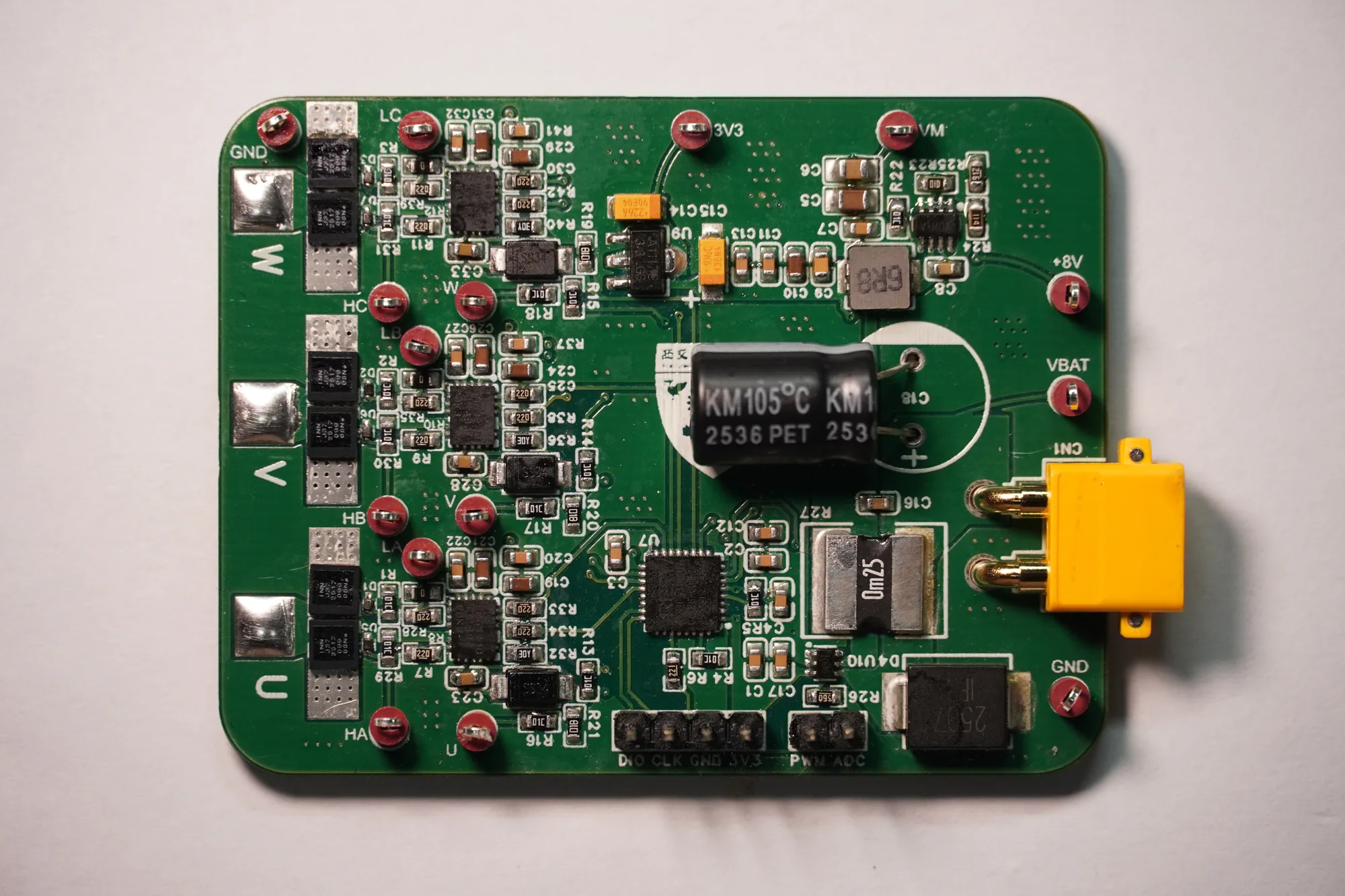
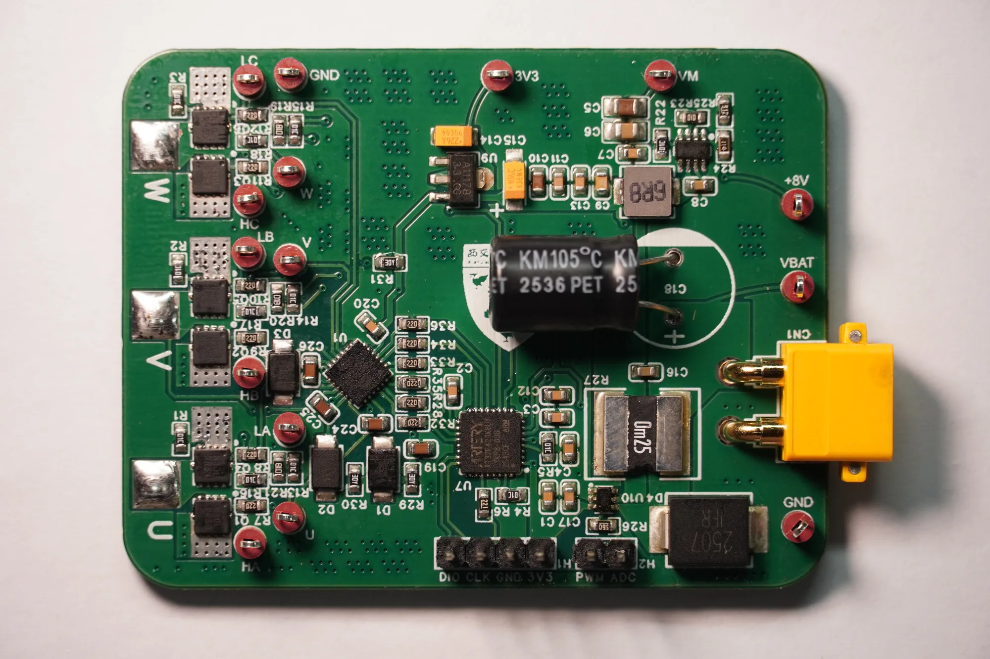
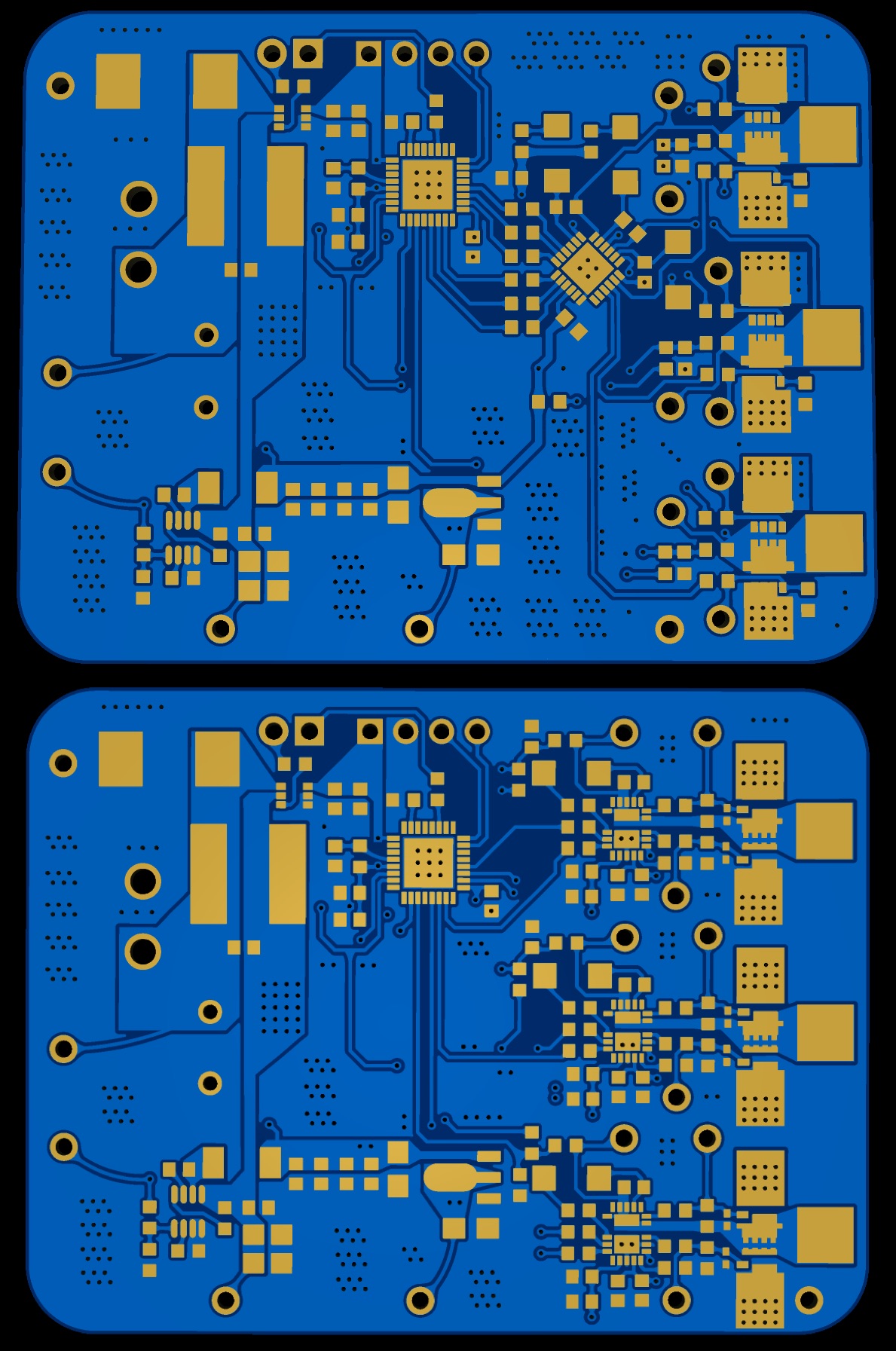
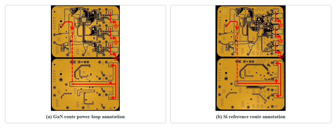
For the comparison to mean anything, the boards had to differ only where they were meant to. They share one overall arrangement, the commutation power loops were drawn as alike as the different packages allowed, and the firmware on the two is practically identical. The second Si revision exists mainly to pull its power routing closer to the GaN layout.
画板的时候,就是奔着对比能说明问题去的。两块板整体布局一致,换流的功率回路在封装不同的前提下尽量画成一个样,两边的固件也几乎一模一样。Si 的第二版重新布线,主要就是为了让它的功率路径更贴近 GaN 板。
Board Revisions and Assembly打板迭代与焊接
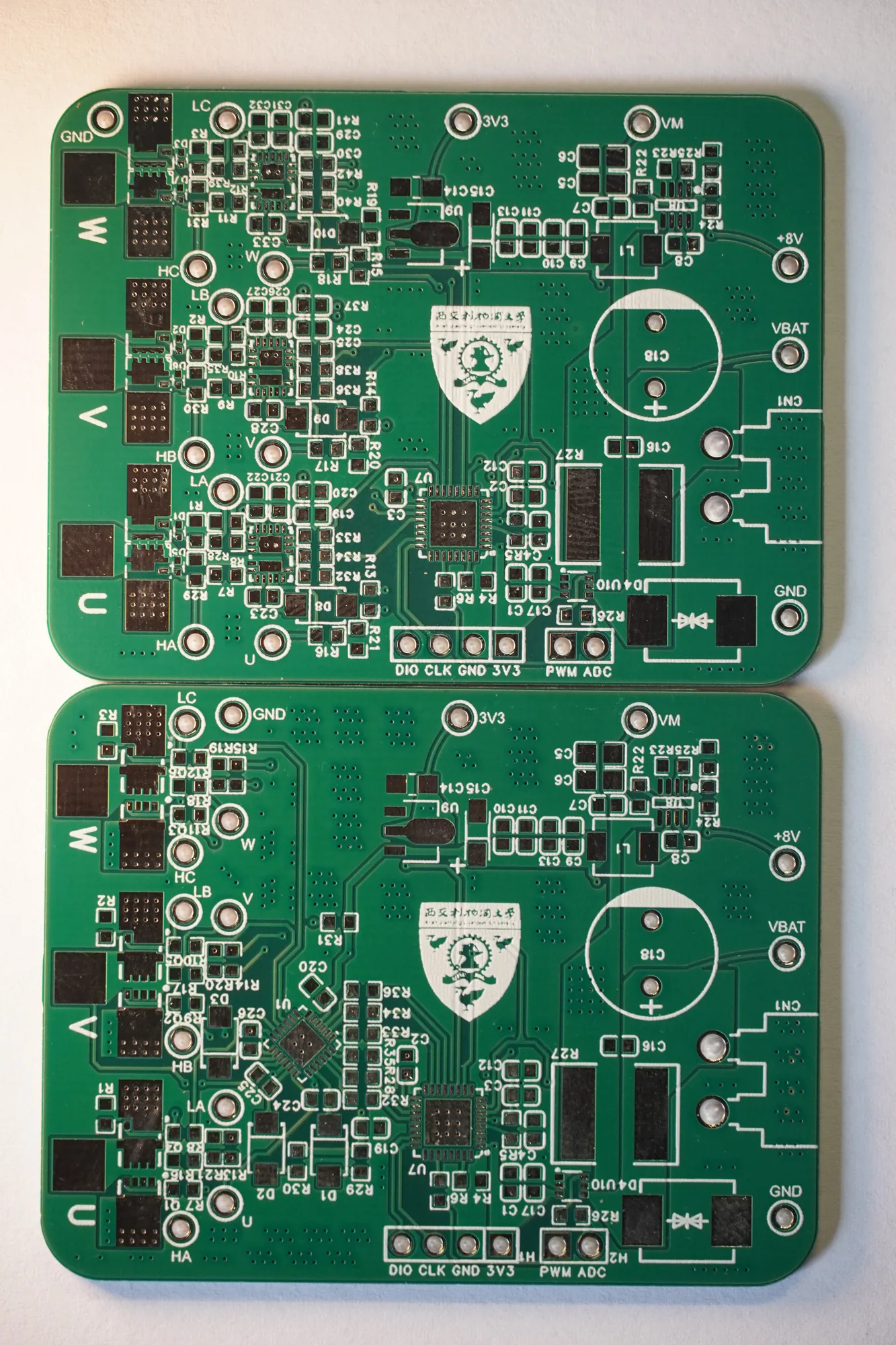
My original plan was cheerfully short: pick the parts, draw the board, spin a motor, write the thesis, graduate. Five board orders later, three GaN and two Si, I knew better. The first GaN board, 1.6 mm thick, saw me through the interim poster. The Si board went from 1.6 mm on its first spin to 1.0 mm on its second, so the GaN board followed with a 1.0 mm revision to keep the comparison fair. What I had never budgeted for was the hardware cycle. Any change meant another four-layer order, a stencil, a parts order and hand assembly, ten days at the very least, and three revisions quietly swallowed over a month.
一开始我脑子里想得特别轻松,器件选好,板子一画,电机一测,论文一写,顺利毕业。结果前前后后打了五次板,GaN 三版,Si 两版。GaN 第一版板厚 1.6 mm,撑过了中期的 poster;Si 第一版也是 1.6 mm,第二版改成了 1.0 mm,为了对比公平,GaN 第二版跟着改成 1.0 mm。真正没算进去的是硬件的研发周期。想改一个地方,就要下一次四层板的订单,再开钢网、买器件、到手自己贴,前前后后怎么也得十天,改三版一个多月就没了。
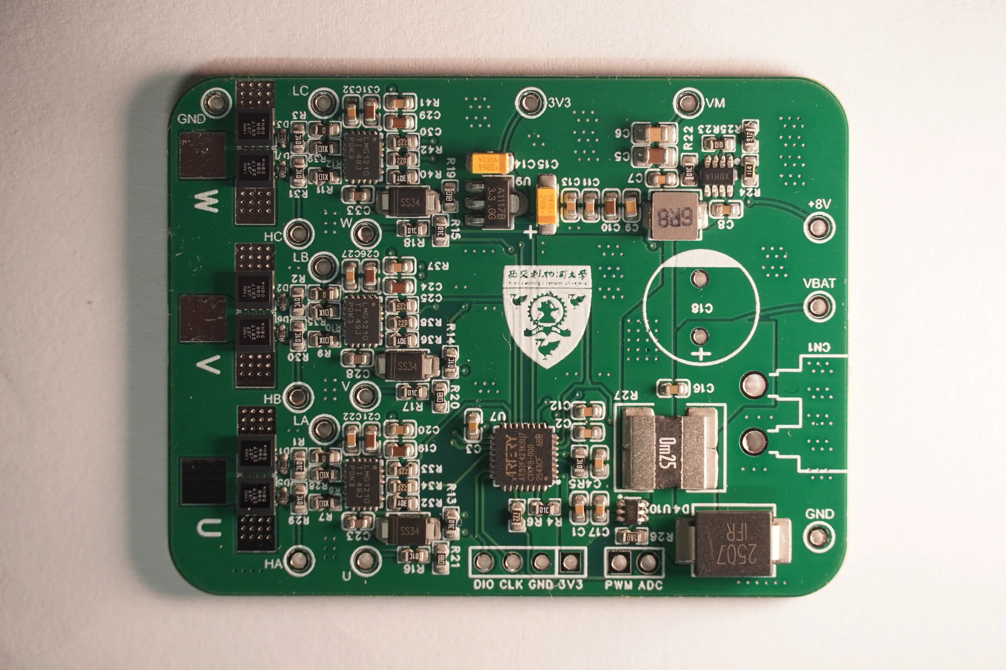
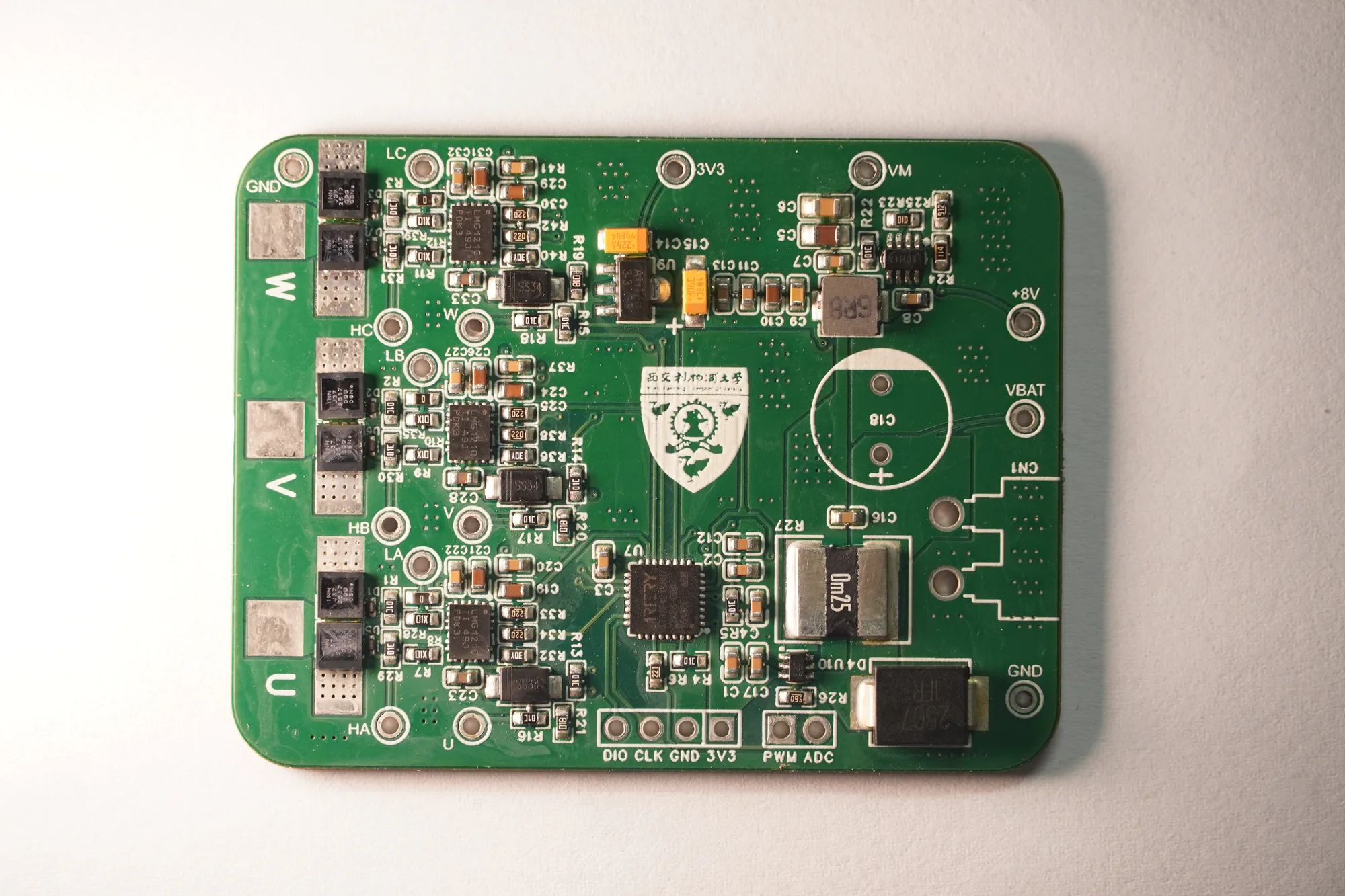
QFN packages were new to me too, and hand soldering them simply did not work. So it became a stencil and solder paste, every part placed by hand, a crash course in what a reflow temperature profile should look like, and a hot plate on which I followed that profile manually. Even then, uneven paste on the Si board's first try bridged pins on the AT32's QFN; solder wick took off the excess and the iron re-tinned the pads. On another board, halfway through soldering, a Bilibili video persuaded me that a 35 V, 470 µF bulk capacitor would handle transients better than the 220 µF in my BOM, so the bigger one went on.
这也是我第一次正经碰 QFN 封装,手焊怎么都焊不好。后来上了钢网刷锡膏,每一颗手工贴上去,还专门学了回流焊的温度曲线该长什么样,再拿加热台手动去模拟。Si 板第一次刷锡膏没刷匀,AT32 的 QFN 引脚回流后连了锡,只好用吸锡带吸掉多余的锡,再用烙铁头蘸一点锡把焊盘重新带一遍。焊另一块板焊到一半,刷 B 站看到母线电容换成 35 V、470 µF 能更好地改善瞬态,就把 BOM 里的 220 µF 换掉了。
On the first GaN board, the LMG1210's bootstrap waveform came out distorted on every measurement. I had calculated the bootstrap capacitor myself, got a figure of one or two hundred nanofarads, and fitted 220 nF on the assumption that it would do. It charged fast and drained just as fast. A 1 µF part fixed the waveform with no change to the layout. Choosing a value barely above the calculation, with no real margin, was the mistake I paid for, and the bootstrap capacitor note works through why a number that looked sufficient on paper fell short on the board.
GaN 第一版上,LMG1210 的自举波形用示波器怎么测都是失真的。自举电容是我自己算的,算出来一两百纳法,就挑了颗 220 nF,想当然觉得够了。结果它充得很快,放得也很快,一下就放光了。换成 1 µF 以后波形就正常了,只换器件,没改版。选值只比算出来的大一点、没留余量,这一堑算是吃了。算出来明明够、装上去却不够,原因放在自举电容这篇笔记里展开。
Shoot-Through Failure上下管直通炸板
The second GaN board is the one I will never forget. I was testing it on a 4S drone LiPo through the XT30 when a high side and low side conducted together. Dead time was set in the firmware, so my suspects were counterfeit parts, a weak spot in the layout, or the MCU running away for a few microseconds before the watchdog dragged it back. A drone pack will hand over a huge current without hesitation. Before I could react, the GaN FET glowed like an LED for perhaps a hundred milliseconds, then went off with a bang, shot about a metre into the air and landed on the desk, thankfully not on me. Its pads took three or four millimetres of copper and solder mask with them in every direction, exposing bare FR-4. I pulled the power far too late, and my first thought was that I would not graduate.
最忘不掉的是 GaN 第二版。那次用 4S 航模电池从 XT30 供电做实验,上下管直通了。死区我是设了的,所以怀疑过买到了假芯片,怀疑过 layout 不够好,也怀疑过单片机突然跑飞几微秒,又被看门狗拉了回来。航模电池给起电流来毫不犹豫。还没等我反应过来,那颗氮化镓管子就跟 LED 一样,啪地亮了大概一百毫秒,然后砰的一声炸飞起来,飞了一米来高,掉在桌上,幸亏没碰到我。管子焊盘周围三四毫米的铜皮连着阻焊一起被扯了下来,直接露出底下 FR-4 的颜色。我反应过来把电拔了,已经晚了,当时第一个念头就是,完蛋,我毕不了业了。
The only protection on the board then was a single bidirectional TVS at the XT30 input. The 5 V bidirectional TVS diodes on the GaN gates did earn their place: that time only one phase's FETs died, while the gates and the other two phases came through. Shoot-throughs in general were far less selective. As I understood it, once a leg shorts, the battery voltage pushes backwards into the DC-DC converter, which has no reverse protection, and then through the ground into the gate drivers and even the controller. Over the whole project I burned three or four AT32s, a good handful of power FETs, two DC-DC chips and two or three LDOs, and the tantalum capacitor beside the LDO briefly became an LED of its own. A little box next to the heat mat on my bench slowly filled with dead chips, some charred black, some missing a corner that had turned to cinders.
那时候板子上只有 XT30 入口一颗双向 TVS,别的保护一概没有。好在 GaN 的栅极上放了 5 V 双向 TVS,那一次只炸了一相的管子,栅极和另外两相都没事。直通一次,坏掉的往往远不止一颗管子。按我当时的理解,桥臂一短路,十几伏的电压会逆着灌进没有反向保护的 DC-DC,再顺着地往驱动芯片甚至主控里灌。整个项目下来,AT32 烧了三四片,功率管烧了好几颗,DC-DC 芯片烧了两块,LDO 烧了两三块,LDO 旁边那颗钽电容在反灌的时候直接变身成一颗 LED,亮了。工作台隔热垫旁边有个小盒,慢慢攒了一堆烧坏的芯片,有的黑得看不清丝印,有的角上烧成了炭渣。
Counting back, nine in ten of those blown transistors died at the same moment: I pushed the throttle up on the test controller, and the propeller-loaded motor had to start from standstill and pull hard for torque. At first I ran AM32 on its default parameters, and its startup yanked torque up so violently that current sloshed between the phases and the transistors simply blew. AM32 exposes a long list of startup settings, among them PWM frequency, complementary PWM, sinusoidal soft start and startup power. Following a blog written by drone hobbyists, I tuned a new set and settled on 48 kHz complementary PWM, sine startup and a startup power of 60, after which blow-ups became far rarer. Why startup is the riskiest moment, and what each of those parameters controls, is in the propeller startup note.
回头一数,九成的炸管都出在同一个时刻:我在上位机里把油门往上推,带着螺旋桨的电机从零开始起转,扭矩一下子拉起来的那一瞬间。一开始 AM32 我用的是默认参数,起转拉扭矩特别暴力,相与相之间的电流乱窜,管子直接就炸了。AM32 里能调的启动参数很多,PWM 频率、用不用互补 PWM、用不用正弦缓启动、启动功率给多大,都能改。后来照着网上玩无人机的人写的博客重新调了一组,最后定在 48 kHz 互补 PWM、正弦启动、启动功率 60,炸管的次数就少了很多。起转那一下为什么最危险、这几个参数各管什么,写在带桨起转这篇笔记里。
Ten and fifteen amp automotive fuses went in series with the input after that, so the fuse goes before the board does. They saved my boards more than ten times and I burned through a whole handful of them; whoever invented the fuse deserves my personal thanks. With the defense about a week away, I placed a 48-hour rush order with JLCPCB for a third GaN board, and that board ran every remaining experiment without a single failure. The rush fee was not cheap and the university would not reimburse it (cue tears), but I am still grateful to JLCPCB. The shoot-through note follows where that fault current goes and what each added protection actually covers.
后来我在入口串上了 10 A 和 15 A 的汽车保险丝,直通那一瞬间保险丝先熔断,板子就保住了。这些保险丝前前后后救了我的板子至少十次,烧掉的保险丝也攒了一大把,我真得好好感谢发明保险丝的人。离答辩只剩一周左右,我找嘉立创加急 48 小时打了 GaN 第三版,这一版从头撑到尾,一次没炸,后面的实验全靠它。加急真的很贵,学校还不给报销(哭),不过还是非常感谢嘉立创。直通的电流到底怎么走、后来加的保护各管哪一段,放在直通与保护这篇笔记里。
Firmware and Flashing固件移植与烧录
Both ESCs run AM32, the open-source ESC firmware, ported to my AT32F421 boards. The official AT32F421 route installs a bootloader first and then loads firmware over a one-wire serial link through a USB adapter. My boards had nothing but a four-pin SWD header, because I had wanted the ESC to stay a pure ESC with a single throttle input, and only at this point did that decision turn awkward. The fix was to move the application to the start of flash, change the vector table offset to match, and flash every build directly over SWD with a DAPLink probe, driven by OpenOCD from VS Code. The AM32 port note has the details, and the ported firmware plus all four test controllers live in STM32-BLDC-ESC-Experiments.
两块电调跑的都是开源电调固件 AM32,我把它移植到了自己的 AT32F421 板上。官方的 AT32F421 方案是先烧一个 bootloader,再用 USB 转串口当单线串口,把固件烧进去,可我的板子上只留了 4 线的 SWD 接口。当初觉得电调就该纯粹,留一个油门输入就够了,到这一步才发现官方的烧录路线走不通,挺尴尬的。最后把程序入口挪到 Flash 起始地址,向量表偏移跟着改,所有固件都用 DAPLink 走 SWD 直接烧,在 VS Code 里配 OpenOCD 一键编译、烧录、调试。具体怎么改的写在 AM32 移植这篇笔记里,移植后的固件和四个测试控制器的代码都在 STM32-BLDC-ESC-Experiments。
Same-Speed Test Method同转速对比方法
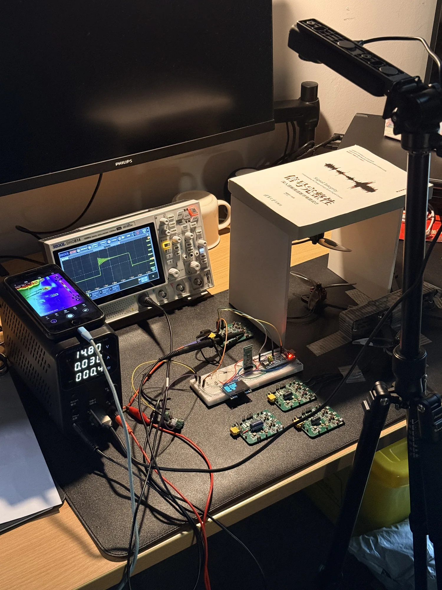
Early tests without a propeller told me almost nothing. With the same motor running unloaded, the two boards differed by so little that neither my tachometer nor the lab oscilloscope could resolve it, and I had no torque sensor, inertia rig or balancing equipment to dig further. The deciding argument was simpler than any of that: a drone never flies without its propellers. If the experiment was meant to describe the real application, the propeller had to go on rather than be left off for the convenience of comparison. Every final test therefore used a KonKer Cler Sky 2207.5 motor and a Gemfan 5128 propeller on a 14.8 V bench supply.
早期做过不带桨的测试,几乎比不出东西。同一个电机、空载的时候,两块板的差别小到我手上的转速计和实验室的示波器都分辨不出来,我也没有测转矩、转动惯量和动平衡的设备。更根本的一点是,无人机在天上飞,就没有不带桨的时候。实验要贴着真实场景做,不能为了对比而对比,所以螺旋桨必须装上。最终实验统一用 KonKer Cler Sky 2207.5 电机、Gemfan 5128 螺旋桨,台式电源供 14.8 V。
The STM32 test controller started life on a USB cable to my laptop. Once the bench moved too far from the computer for any serial cable I owned, I added an HC-05 Bluetooth module and changed the controller firmware so the laptop could start and stop each run remotely, which also kept me well away from a spinning propeller. On the laptop, VOFA+ received the serial stream and plotted it live. I rate it extremely highly and recommend it to anyone debugging embedded hardware over a serial port.
STM32 测试控制器一开始是用 USB 线直接插在电脑上的。后来实验台离电脑太远,中间传串口数据的线不够长,就补了一个 HC-05 蓝牙模块,上位机程序也跟着改,电脑可以远程控制它启动和停止每一轮实验,人离转着的螺旋桨远一点,也更安全。电脑这头用 VOFA+ 接收串口数据、实时画曲线,这个软件我的评价是非常夯,推荐给所有靠串口调嵌入式的人。
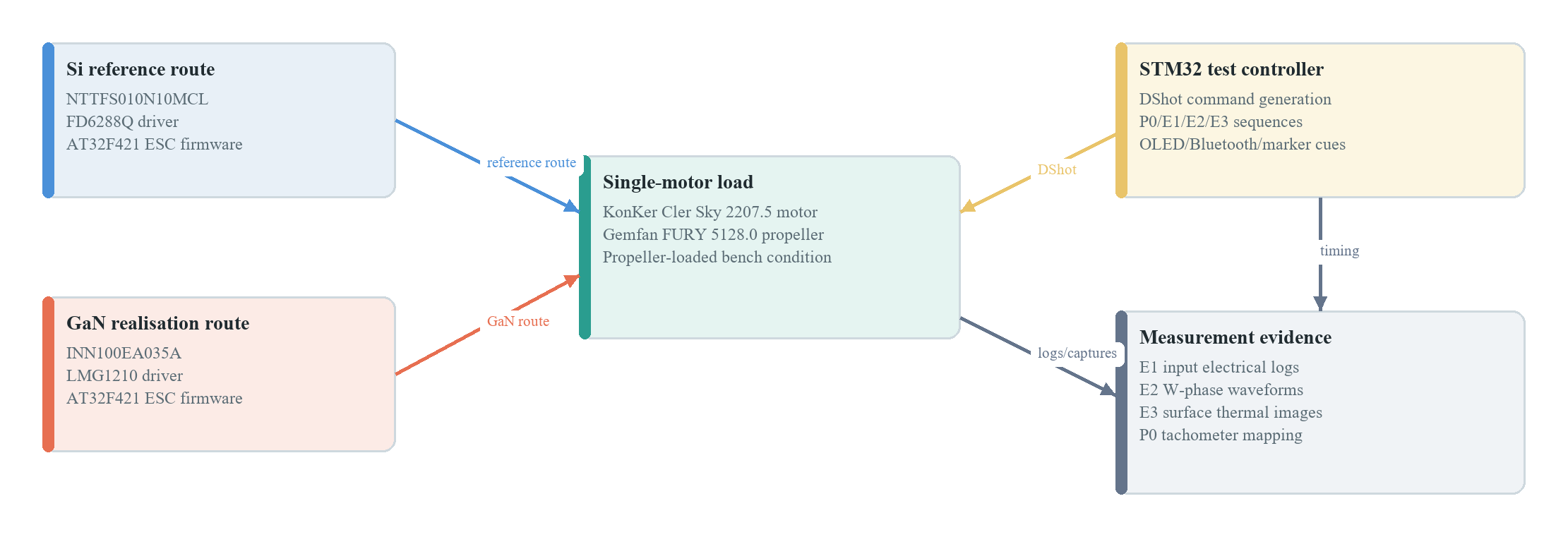
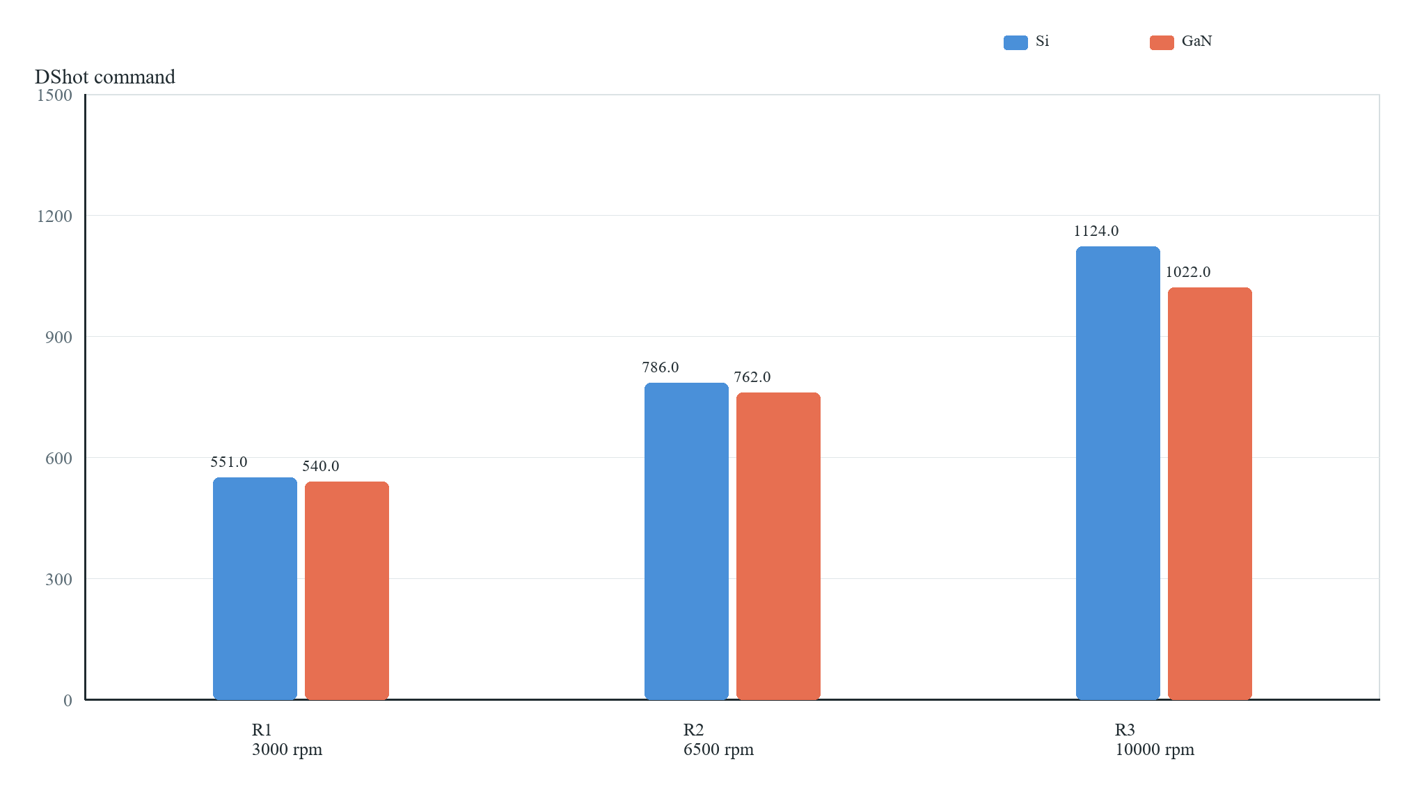
The propeller brought its own problem. Given the same DShot throttle value from the STM32 test controller, the two boards spun it at different speeds, presumably because of their different power devices and drivers. A propeller at a different speed is a different load, with different torque and power, so comparing at equal throttle would have compared two loads. I added a step in front of the main tests, P0, using a tachometer to find the DShot command each board needed for 3000, 6500 and 10000 rpm. With speeds matched, E1 recorded input voltage, current and power, E2 captured the switching waveform at the W phase node, and E3 tracked surface temperature through a 600-second run. The same-speed note covers how the mapping was built and what it lets the later numbers say.
螺旋桨一装上,问题就来了。STM32 测试控制器发出同一个 DShot 油门值,两块电调带着螺旋桨转出来的转速不一样,我估计是功率器件和驱动芯片不同造成的。转速不同,螺旋桨的转矩和要的功率也跟着不同,直接对比等于在比两种负载。于是正式实验前加了一步 P0,用转速计找出两块板分别要多大的 DShot 指令,才能转到 3000、6500 和 10000 rpm。转速对齐了,再做 E1 测输入电压、电流和功率,E2 测 W 相节点的开关波形,E3 测 600 秒里的表面温度。映射具体怎么做、能让后面的数说明什么,写在同转速对比这篇笔记里。
Comparison Results对比结果
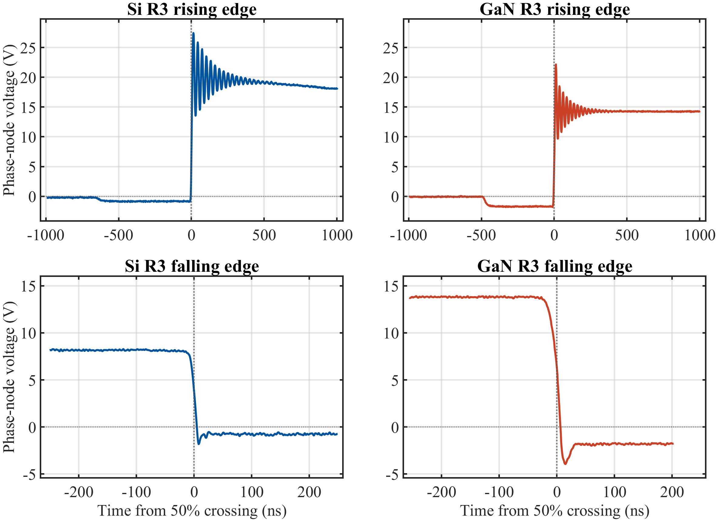
Averaged over three runs at 10000 rpm, the GaN board drew about 27.0 W from the supply against 45.0 W for the Si board; at 6500 rpm the figures were 10.4 W and 15.1 W, and at 3000 rpm 2.8 W and 3.4 W. On the W phase rising edge at 10000 rpm, overshoot came to about 1.9 V on GaN and 4.0 V on Si, and the ringing settled in about 29 ns on GaN compared with roughly 500 ns on Si. After 600 seconds at 10000 rpm in a 25 °C room, the surface around the V phase transistors read 34.0 °C on the GaN board and 38.9 °C on the Si board.
10000 rpm 时,三次平均下来,GaN 板从电源取了约 27.0 W,Si 板约 45.0 W;6500 rpm 时是 10.4 W 对 15.1 W,3000 rpm 时是 2.8 W 对 3.4 W。10000 rpm 下 W 相的上升沿,GaN 板过冲约 1.9 V,Si 板约 4.0 V;振铃在 GaN 板上约 29 ns 就稳住,Si 板要五百纳秒上下。10000 rpm 连续跑 600 秒后,V 相功率管附近的表面温度,GaN 板 34.0 °C,Si 板 38.9 °C,室温 25 °C。
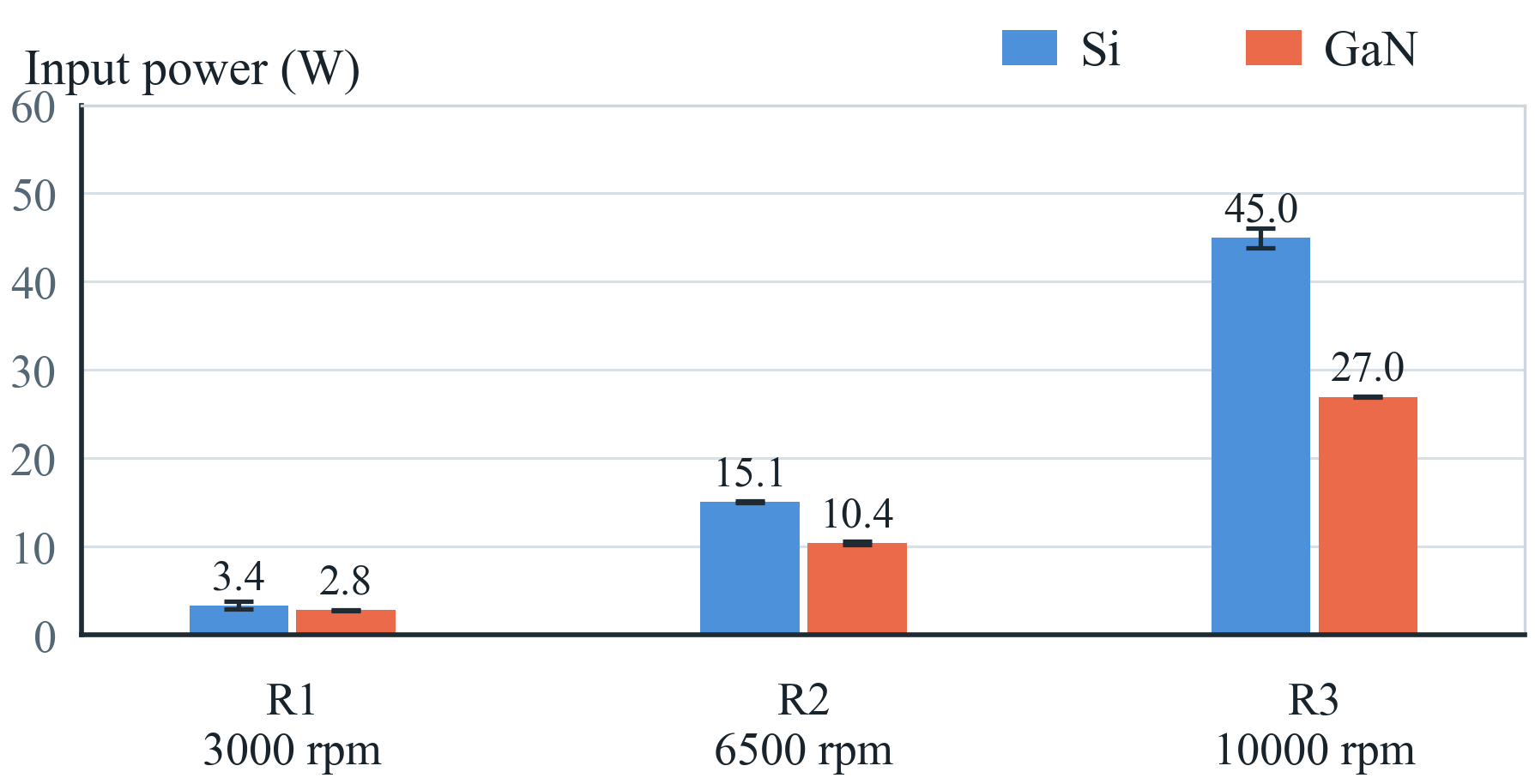
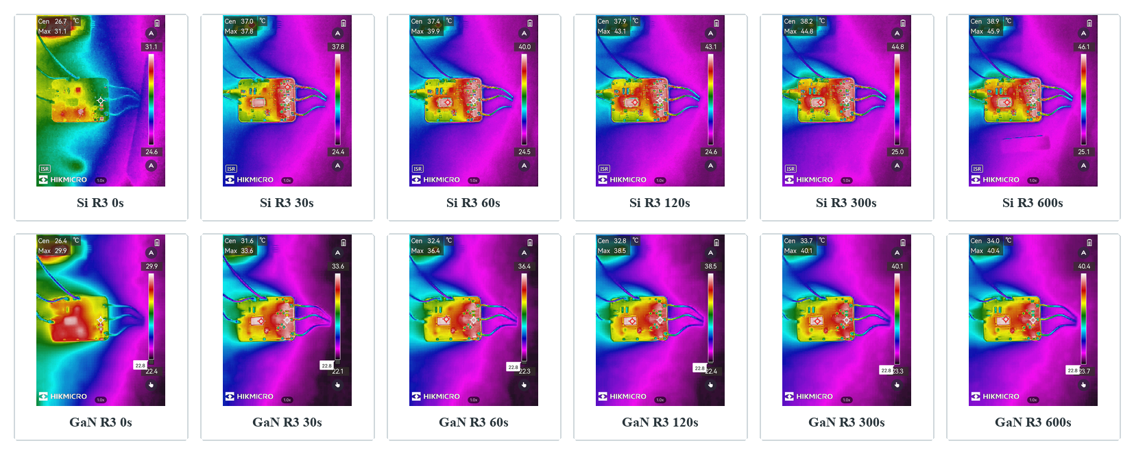
Those numbers arrived like a rescue. Two boards had blown up, I had stopped counting dead transistors, the defense was close, and I was beginning to lose hope. The last pair of boards carried the entire sequence from start to finish, and the gap turned out wider than I had expected, which was a genuine thrill. I also knew exactly what I was holding: input power at matched speed, measured on two boards whose drivers and switches were different to begin with. It pointed the way I expected, only further than I had dared to hope.
看到这组数,我有种劫后余生的感觉。板子炸过两次,烧掉的管子数不过来,答辩又近在眼前,我当时已经有点丧失希望了。最后这两块板硬是把整个实验流程从头撑到了尾,差距还比我预想的大,那种惊喜是真的。惊喜归惊喜,心里也清楚,这是同转速下的输入功率,两块板的驱动芯片和开关管本来就不一样,结果符合预期的方向,也比我期待的更好。
Final Defense and Grade答辩与成绩
Every other undergraduate Prof. Zhang supervised that year built their motor-drive project as a MATLAB Simulink simulation; I was the only one who walked into the defense with real hardware. Only P0 was finished and I was still waiting on the newest board, so I went in on nerve, powered the ESC in front of the panel, spun the propeller through several speeds, and talked through the board comparison, the design, the planned experiments and the timeline. Each slot was supposed to last ten to fifteen minutes, questions included. Mine lasted fifty-five. The slides took ten; for the remaining forty Prof. Zhang kept pointing at my schematic and asking, in English, why this capacitor sat here, why that resistor was there, what this was, what that was. My spoken English was not great back then, so it was a live grilling of the purest kind, and I still remember every minute.
那一年在张老师手下做毕设的本科生,其他人做的都是 MATLAB 里的 Simulink 电驱仿真,只有我一个人真的手搓了硬件带进答辩。那时候实验只做完了 P0,还在等最新的板子,我是硬着头皮上去的,当着老师的面上电,让螺旋桨转出不同的转速,讲了两块板的对比、原理、论文里的实验流程和时间线。学校规定每个人答辩十到十五分钟,讲 PPT 和回答问题都算在里面,我一个人在里面待了五十五分钟。PPT 讲了十分钟,后面四十分钟张老师一直指着我的电路图问,这里为什么放这个电容,那里为什么放这个电阻,这是什么,那又是什么。对当时英语还没那么好的我来说,这就是纯英文现场拷打,非常考验临场发挥,所以印象特别深。
I was second to last. When I came out, the one student still waiting stared at me and asked what had taken so long; I genuinely had no idea. He was done in six minutes and came out to thank me: after fifty-five minutes on me, Prof. Zhang let him through with hardly any questions. Prof. Zhang had told me beforehand not to panic, to defend first and finish the experiments afterwards, and that is how it went: E1 to E3 were done in mid-May and the thesis went in at the end of the month. SAT301, the ten-credit final-year project module, came out at 72. That sits in the 70-plus first-class band of the UK marking scheme XJTLU follows, and my transcript records it as an A.
我是倒数第二个进去的。出来的时候,外面就剩一个同学,他都傻了,问我怎么那么久,我说我也不知道。他进去六分钟就出来了,还特地谢我,说幸亏我拖了张老师那么久,老师没怎么问他就让他过了。我都不知道该说啥。张老师之前就跟我讲过,不用着急,可以先答辩,再把后面的实验补上,事情也确实是这么走的。E1 到 E3 在五月中旬做完,月底交了论文。SAT301 这门十学分的毕设课最后拿了 72 分,在西浦沿用的英式评分里落在 70 分以上的一等区间,成绩单上是 A。
Prof. Zhang backed me from start to finish, through the blown boards and the experiments that ran right up to the deadline. If you are an XJTLU student looking for a final-year supervisor in motor drives or power electronics, I recommend him without hesitation; his profile is on the XJTLU scholar page.
张老师全程都非常支持我,炸板也好,实验拖到最后也好,一直都在。西浦的学弟学妹如果在找电驱或电力电子方向的毕设导师,我真心推荐张老师,他的主页在西浦学者主页上。
Development notes开发笔记
Debugging records and technical notes tied to the decisions and artifacts on this project page.与这个项目页面中的设计决策和工程材料直接关联的调试记录与技术笔记。
- 01AM32 on AT32F421 Without a Bootloader去掉 bootloader 的 AT32F421 版 AM32Why the official AM32 layout starts the application at 0x08001000, and what had to change in the linker script, scatter file and vector table offset to flash it directly over SWD.官方 AM32 为什么把程序放在 0x08001000,以及要通过 SWD 直接烧录时,链接脚本、scatter 文件和向量表偏移各要改什么。
- 02LMG1210 Bootstrap Capacitor SizingLMG1210 自举电容选型A 220 nF bootstrap capacitor that matched the datasheet formula still distorted the GaN ESC's high-side waveform. Working the formula through a six-step ESC's floating phase shows where the missing charge went.按手册公式算出来够用的 220 nF 自举电容,装上 GaN 电调后高边波形还是失真。把公式放进六步换相里一相悬空的那段时间再算一遍,缺的电荷就找到了。
- 03Propeller-Loaded Startup and AM32 Startup Parameters带桨起转与 AM32 启动参数Most blown transistors on the GaN ESC died the moment a propeller-loaded motor started from standstill. Why that moment draws so much current in a sensorless six-step drive, and what AM32's startup power, sine startup and stall protection settings each control.GaN 电调的炸管大多出在带桨电机从静止起转的那一下。无感六步驱动里,这一下为什么电流最大,以及 AM32 的启动功率、正弦启动和堵转补偿这几项参数各自管什么。
- 04Same-Speed Comparison and DShot Mapping同转速对比与 DShot 转速映射With a propeller fitted, one DShot throttle value spun the GaN and Si ESCs at different speeds. Why that breaks a direct comparison, and how the P0 tachometer mapping matched both boards at 3000, 6500 and 10000 rpm.装上螺旋桨以后,同一个 DShot 油门值让 GaN 和 Si 两块电调转出了不同的转速。为什么这样没法直接比,以及 P0 怎样用转速计把两块板对齐到 3000、6500 和 10000 rpm。
- 05Shoot-Through Current Paths and Protection上下管直通的电流路径与保护Shoot-throughs on the GaN ESC killed far more than the power transistors. Following the fault current through the bus, the ground and the gates shows what the dead time, gate TVS, input fuses and input TVS each protect, and where a gap remains.GaN 电调的几次直通,坏掉的远不止功率管。顺着故障电流走一遍母线、地和栅极,看清死区、栅极 TVS、入口保险丝和入口 TVS 各自护住的是哪一段,又在哪里留了空档。
Public Project Files公开项目资料
Uploaded evidence served from the public asset folder. Use the file index to preview documents, source code, media, PDFs, and downloadable artifacts without leaving the page.这里列出已经上传到公开目录的项目证据。可以在左侧索引里选择文件,在右侧直接预览文档、源码、媒体、PDF 和可下载附件。
e1-measurement-limitations.txt
Text / 2.2 KB
E1 measurement limitations Date: 2026-05-18
This folder records final propeller-loaded same-RPM E1 steady-state electrical evidence. The processed tables report input-side electrical behaviour derived from the STM32 E1 controller logs: VBAT, input current, and input electrical power.
Allowed interpretation: - The E1 data can support statements about measured/processed input voltage, input current, input power, voltage sag, and repeatability at the selected P0 same-RPM operating points. - The E1 data can be compared at the recorded R1/R2/R3 target-speed conditions because the DShot commands were selected from the P0 tachometer mapping. - The repeated run cycles can be used as repeatability evidence for the input electrical telemetry under the same logged setup.
Important limitations: - Input electrical power is not strict ESC efficiency. - The E1 logs do not include torque, thrust, shaft power, aerodynamic output, or mechanical output power. - Same-RPM input electrical comparison does not prove equal thrust, equal torque, or equal useful propulsive output. - The data were collected on the local propeller-loaded bench setup, not on a calibrated dynamometer. - Current and voltage values are firmware-processed telemetry values from the ADC/INA199/VBAT-divider measurement chain; final thesis wording should mention calibration and uncertainty limitations unless separate calibration evidence is added. - DShot command differences between Si and GaN boards are operating-point selection evidence only, not performance evidence by themselves. - Any conclusion about lower loss, higher efficiency, thermal superiority, flight performance, or commercial reliability requires additional evidence beyond this E1 folder.
Recommended thesis wording: - Safe: "The E1 experiment reports input electrical behaviour at P0-selected propeller-loaded same-RPM operating points." - Safe: "The processed input power is treated as an input-side electrical quantity, not as complete ESC efficiency." - Unsafe: "The GaN route is more efficient" unless supported by torque/thrust/shaft-power or other matched-output evidence. - Unsafe: "The same-RPM points prove equal mechanical output" because RPM alone does not establish torque or thrust.
Related media相关媒体
Board photos, schematic sheets, videos, and test captures that show this project at specific stages.展示这个项目具体阶段的板卡照片、原理图分页、视频和测试截图。
Final GaN ESC, assembled组装完成的 GaN 电调Final Si reference ESC, assembled组装完成的 Si 参考电调Bare Si and GaN boardsSi 与 GaN 裸板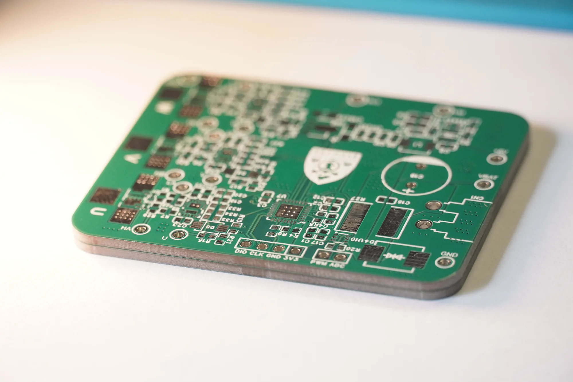 Board size comparison两块板的尺寸对比Placing parts on stencilled paste在钢网锡膏上贴片GaN board after hot-plate reflow加热台回流后的 GaN 板
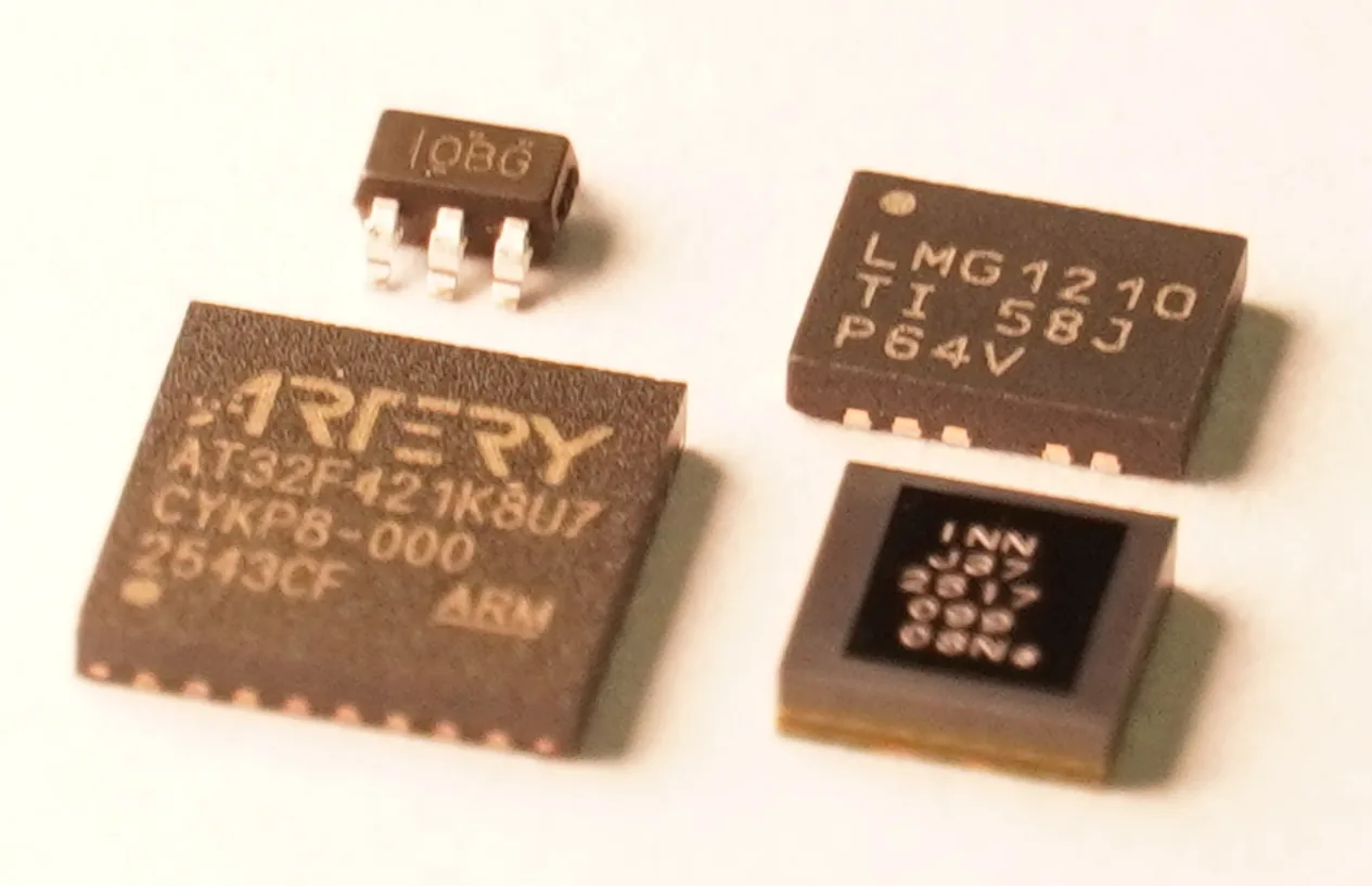 GaN route key partsGaN 路线的关键器件Propeller-loaded test bench带桨测试台
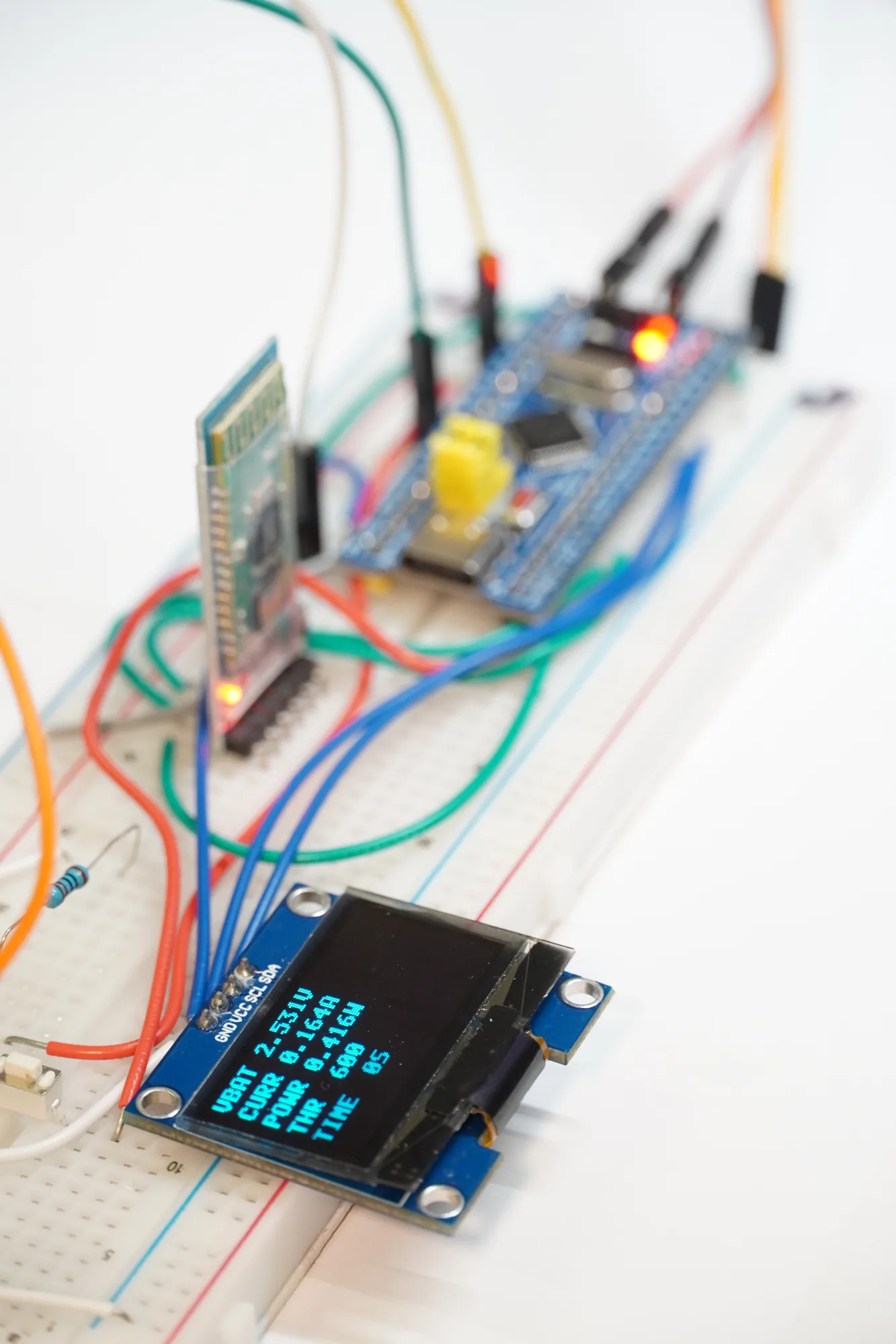 STM32 test controllerSTM32 测试控制器
 GaN ESC PCB renderGaN 电调 PCB 渲染Si and GaN layoutsSi 与 GaN 的布局Annotated power loops功率回路标注Comparison setup对比实验的系统结构
 DShot commands for matched speed对齐转速所需的 DShot 指令Input power at matched speed同转速下的输入功率W-phase switching edges at 10000 rpm10000 rpm 下的 W 相开关边沿Thermal sequence at 10000 rpm10000 rpm 热像序列