

2026-09-07
A Switched Battery Divider and ADC Settling电池采样开关与 ADC 建立时间
Calculating the settling, current consumption and error sources of the Claude Chime battery-voltage divider.从 Claude Chime 的受控分压电路出发,计算建立时间、采样耗电与电压换算误差。
My Claude Chime software handoff recommends enabling ADC_ENABLE, waiting 5 to 10 ms, taking several readings and then disabling the divider. The voltage conversion uses just one ratio, so why the wait? The capacitor next to the ADC input supplies the explanation.
我给 Claude Chime 写的软件交接文档里,电池采样顺序是拉高 ADC_ENABLE,等待 5 到 10 ms,多次读取,再关闭采样支路。分压公式只有一个系数,为什么还要等?答案要从 ADC 引脚旁边那颗电容说起。
Divider and Switch分压与开关
In the schematic, an AO3401 high-side switch connects the battery to a divider formed by 15 kΩ and 22 kΩ resistors. Driving ADC_ENABLE high turns on a 2N7002, which pulls the AO3401 gate low and enables the branch. A further 1 kΩ resistor connects the divider midpoint to ADC_BAT, where a 100 nF capacitor goes to ground.
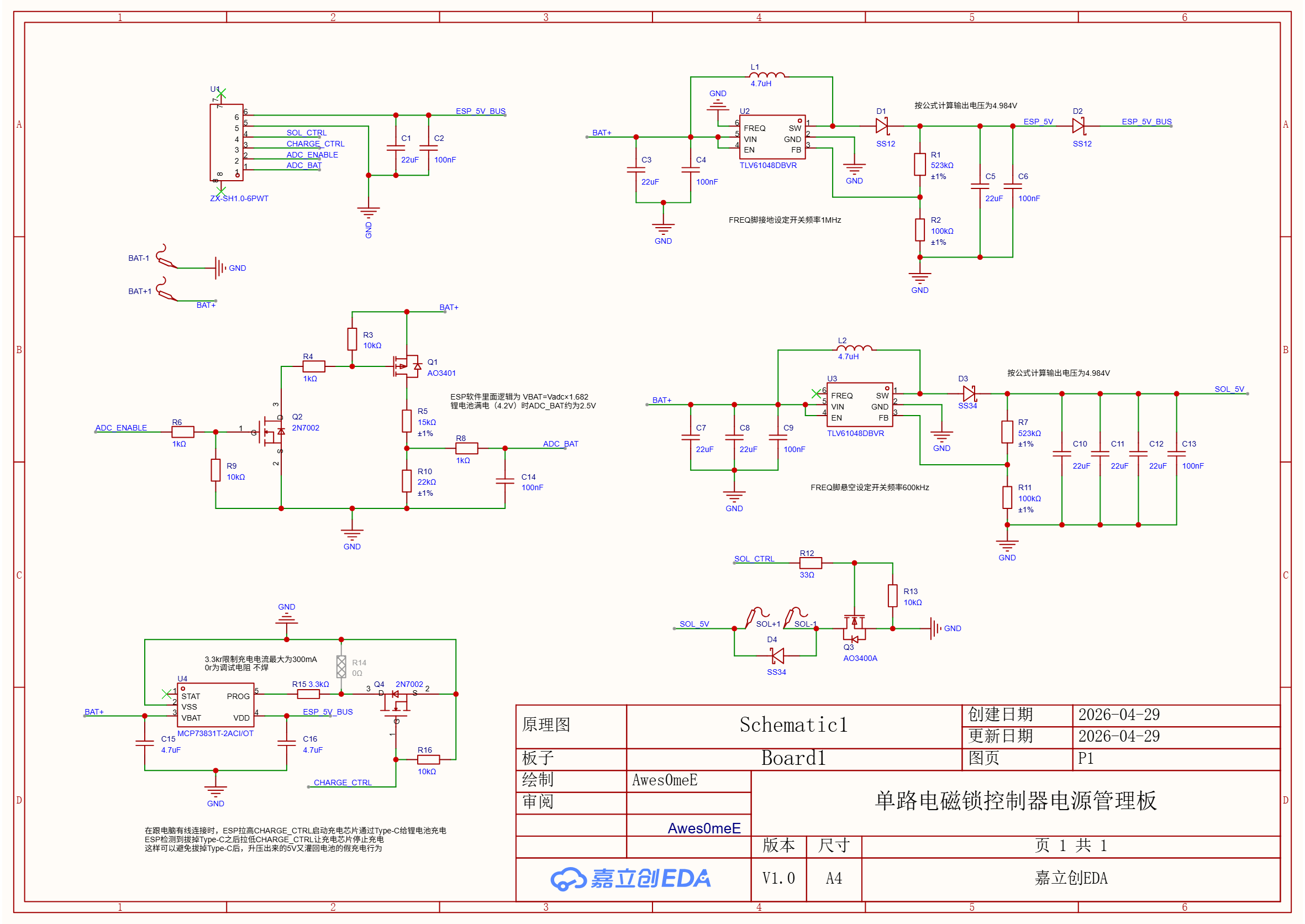
在原理图中,电池通过 AO3401 高侧开关给分压支路供电,15 kΩ 与 22 kΩ 电阻负责分压。ADC_ENABLE 拉高以后,2N7002 导通,把 AO3401 的栅极拉低,分压支路才接通。分压节点经过 1 kΩ 电阻接到 ADC_BAT,ADC 侧还有一颗 100 nF 对地电容。
Ignoring switch resistance and ADC input current, the settled output is VADC = VBAT × 22 / 37, giving the inverse ratio 37 / 22 ≈ 1.682. A 4.2 V battery therefore produces a target of about 2.497 V at the ADC node. At enable time, however, the 100 nF capacitor has to charge before that voltage is reached.
在稳定状态下,先忽略开关导通电阻和 ADC 输入电流,分压输出为 VADC = VBAT × 22 / 37,反算系数为 37 / 22 ≈ 1.682。电池电压取 4.2 V 时,ADC 节点的目标电压约为 2.497 V。但刚接通的瞬间,100 nF 电容需要充电,电压要经过一段时间才接近这个目标。
RC Settling TimeRC 电路的建立时间
To calculate the resistance seen by the capacitor, I set the ideal voltage source to zero in the circuit model. The 15 kΩ and 22 kΩ resistors are then in parallel, followed by 1 kΩ in series. The resulting Thevenin resistance is about 9.919 kΩ. With 100 nF, the time constant is approximately 0.992 ms. For a capacitor starting at 0 V, the first-order remaining-error fraction is exp(-t/τ).
计算前级电路的戴维南电阻时,先在电路模型中把理想电压源置零。15 kΩ 与 22 kΩ 因而并联,再与 1 kΩ 串联,得到约 9.919 kΩ 的等效电阻。配上 100 nF,时间常数约为 0.992 ms。假设电容从 0 V 开始充电,一阶模型中的剩余误差比例为 exp(-t/τ)。
| Wait | Remaining error | Equivalent error magnitude at a 4.2 V battery |
|---|---|---|
| 1 ms | About 36.5% | About 1.53 V |
| 5 ms | About 0.647% | About 27.2 mV |
| 10 ms | About 0.00419% | About 0.176 mV |
| 等待时间 | 剩余误差比例 | 换算到 4.2 V 电池端的误差幅值 |
|---|---|---|
| 1 ms | 约 36.5% | 约 1.53 V |
| 5 ms | 约 0.647% | 约 27.2 mV |
| 10 ms | 约 0.00419% | 约 0.176 mV |
These are ideal RC calculations for settling from zero. A few milliseconds between 5 and 10 ms make a considerable difference. Immediately taking 32 samples and averaging them could simply average a voltage that is still rising.
这张表是理想 RC 计算,只讨论从零建立时的误差。它说明 5 ms 和 10 ms 虽然只差几毫秒,建立程度已经差了很多。接通以后立刻连续读 32 次,再把它们平均,也可能只是在平均一段仍然上升的电压。
Setting an isolated RC settling target of 0.1% requires approximately 6.91τ, or 6.85 ms. Component tolerances, MOS turn-on, ADC sampling load and the required measurement accuracy also affect the chosen wait. The handoff's 5 to 10 ms recommendation can therefore be checked against the node waveform and actual ADC readings before selecting a duration.
如果单独把 RC 建立误差目标设为 0.1%,则需要约 6.91τ,也就是 6.85 ms。实际等待还要考虑电阻电容容差、MOS 开通过程、ADC 采样负载和测量要求。交接时给出的 5 到 10 ms 因而可以继续用示波器与实际 ADC 读数核对,再选择合适的时长。
Sampling-Circuit Current Consumption采样电路的电流消耗
At 4.2 V, the 37 kΩ divider draws about 113.5 μA, or 2.72 mAh over a full day if continuously connected. Switching it on for an illustrative 10 ms each second reduces the average current in the divider resistors alone to about 1.14 μA.
4.2 V 下,37 kΩ 分压支路的静态电流约为 113.5 μA,持续接通一天约消耗 2.72 mAh。开关让它只在测量窗口内工作,例如每秒接通 10 ms,单算分压电阻的平均电流就约为 1.14 μA。
There are other paths to count. The AO3401 gate has a 10 kΩ pull-up. When the 2N7002 conducts, that pull-up and the series 1 kΩ form another path drawing approximately 382 μA at 4.2 V under an ideal on-state approximation. That exceeds the divider current itself. Capacitor recharging, GPIO drive and off-state leakage add further consumption. The divider-resistor calculation is therefore only part of the complete sensing circuit's power budget.
不过,这还没算完整。AO3401 的栅极通过 10 kΩ 上拉,2N7002 导通时,这条上拉与串联 1 kΩ 也形成电流路径。在理想导通近似下,4.2 V 对应约 382 μA,比分压支路本身还大。电容每次充电、GPIO 驱动及关断漏电也各有消耗。评估整套采样电路时,要把这些支路一起算,不能只用分压电阻的电流宣称总功耗。
Conversion time also extends the enabled window. Waiting 10 ms and then spending additional time taking samples produces a duty above 1% when repeated every second. Including that time makes it easier to choose a sampling rate and judge the energy cost of additional readings.
连续采样的耗时同样属于接通窗口。如果等待 10 ms 后又花时间完成多次转换,实际占空比就高于 1%。这样算完,我更容易决定采样频率该多高,以及为了多读几次付出了多少电量。
ADC ConversionADC 换算
ESP32-S3 conversion also involves attenuation and calibration. Espressif's calibration documentation provides raw-code-to-voltage conversion and discusses input capacitance and multisampling for noise reduction. Software should first obtain an input voltage appropriate to the ADC configuration, then apply the divider ratio. A single fixed full-scale formula does not fit every configuration.
ESP32-S3 的 ADC 还涉及衰减设置和校准。Espressif 的校准文档提供原始码到电压的校准接口,也讨论了输入电容和多次采样对噪声的改善。软件应先得到符合当前 ADC 配置的输入电压,再乘分压系数,不能把所有配置都套进一个固定满量程公式。
The error sources need separate treatment. Averaging can reduce some random noise, but cannot automatically remove the consistently low reading caused by incomplete settling. Divider-ratio and ADC-conversion errors can combine as well. Comparing several stable voltages against a meter at low, intermediate and near-full-battery levels reveals more than correcting one point alone.
误差也要分开处理。平均可以降低部分随机噪声,持续偏低的 RC 建立误差却不会自动消失;分压比偏差与 ADC 换算偏差也可能叠加。用几个稳定电压点对照万用表,分别检查低端、中间与接近满电的位置,会比只校准一个点更容易发现差异。
I checked the analog voltage on my bench after manually enabling this circuit; the client's firmware handled the ESP32 readings. Working through the circuit explains why the handoff needed both a control sequence and a conversion ratio. Enabling the switch, allowing settling, acquiring samples and calibrating them all contribute to a battery reading that can usefully guide the next operation.
这块板在我的桌上做过手动使能后的模拟电压检查,ESP32 的实际读取由客户固件负责。沿电路继续计算以后,我更清楚交接时为什么要同时写出控制顺序与换算关系。一次电池读数要经历开关接通、电压建立、ADC 采样和校准换算,等这些动作配合好了,屏幕上的电压才值得用来判断下一步操作。