

Claude Chime Power BoardClaude Chime 电源板
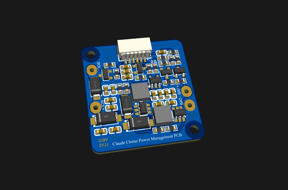
For an independent hardware commission from Accele AI, I designed and hand-assembled Claude Chime's ESP32 peripheral power board. The roughly 28 × 27 mm PCB combines single-cell charging, two separate boost rails, gated battery-voltage sensing, and a 5 V push-pull solenoid driver. I completed basic power-up and interface checks; the client's firmware engineer later reported normal complete-device operation.受 Accele AI 委托,我独立设计并手工焊接了 Claude Chime 的 ESP32 外围电源板。约 28 × 27 mm 的 PCB 集成单节锂电池充电、两路独立升压、受控电池电压采样和 5 V 推拉式电磁铁驱动。我完成了基础上电与接口测试,客户固件工程师随后反馈整机运行正常。
- Timeline时间线
- 2026.04 - 2026.052026.04 - 2026.05
- Status状态
- Commissioned Hardware委托硬件项目
- Stack技术栈
- PCBPower ElectronicsESP32-S3BatteryBoost ConverterHardware Bring-up

Solenoid Drive电磁铁驱动
A few jumps from a desktop crab announce that Claude has finished a task on the computer. That is the idea behind Accele AI's Claude Chime: make the reminder noticeable even to someone looking down at a phone. The crab is a 3D-printed Clawdy Family model, moved by a 5 V push-pull solenoid under ESP32 control.
电脑里的 Claude 干完活,桌上的螃蟹就跳几下。Accele AI 的 Claude Chime 想用这种动静,让低头看手机的人也能注意到任务已经完成。螃蟹是 Clawdy Family 的 3D 打印模型,动作由 ESP32 控制的 5 V 推拉式电磁铁完成。
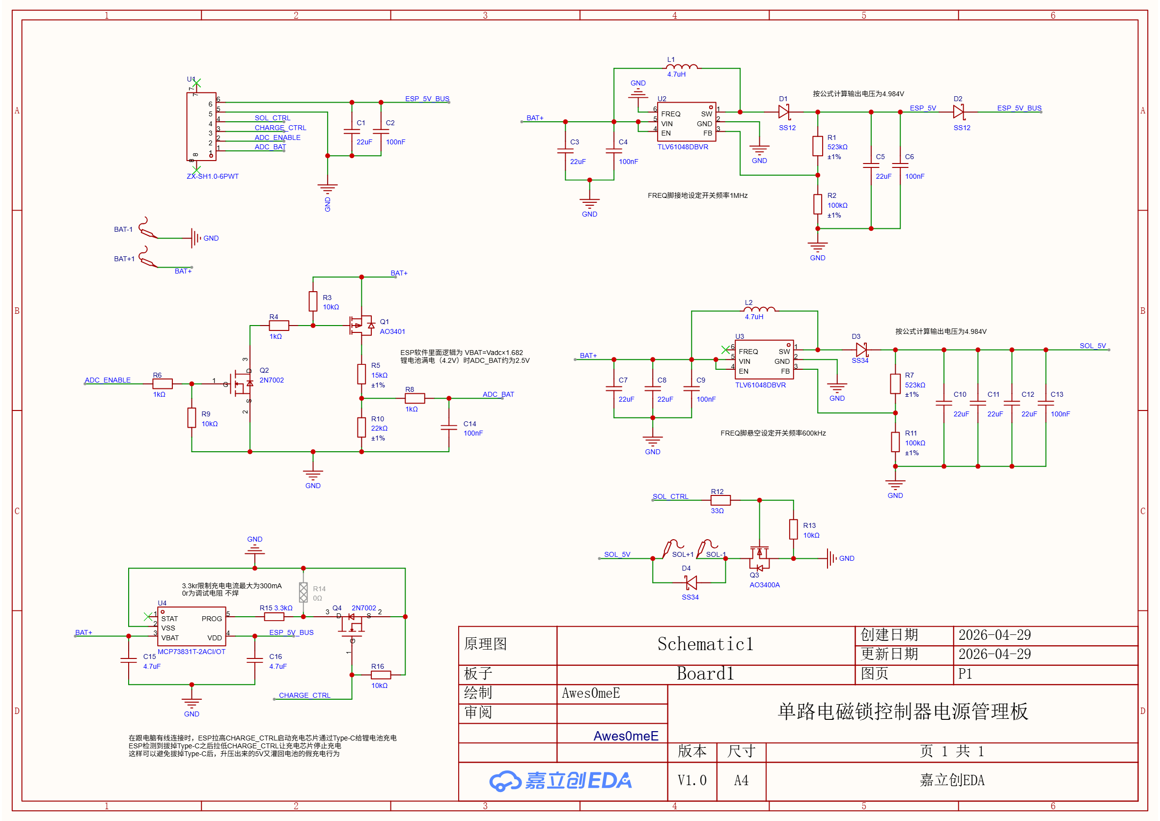
Accele AI commissioned me to develop the hardware independently. Their initial proposal used a relay for the solenoid, but enclosure space led me to a low-side MOSFET instead. SOL_CTRL drives an AO3400A through a 33 Ω gate resistor, with a 10 kΩ pull-down keeping it off by default. An SS34 provides the flyback path when the solenoid is switched off. The smaller switching circuit was a better fit inside the crab.
我接下的是这套装置的付费独立硬件委托。对方起初想用继电器控制电磁铁,我考虑到外壳里的空间,把驱动改成了低边 MOSFET。SOL_CTRL 通过 33 Ω 栅极电阻控制 AO3400A,10 kΩ 下拉电阻保证默认关断,SS34 则在电磁铁断电时提供续流路径。这套开关电路占的空间更小,更适合螃蟹的外壳。
Battery operation made the job broader. The device needed to run without a power cable, charge a single lithium-ion cell, and work with the client's existing ESP32-S3 core board. I had to account for power with Type-C connected, battery takeover when it was unplugged, and the effect of solenoid actuation on the controller. I needed to work through those states as part of the circuit design.
但设备还要脱离电源线运行,要给单节锂电池充电,又必须沿用客户现成的 ESP32-S3 核心板。我得继续想清楚,插着 Type-C 时怎么供电,拔掉以后谁来接手,电磁铁动作时又会不会影响主控。开关电路之外,这几种工作状态也得一起设计。
Two Boost Rails两路升压
During selection, I considered integrated power devices such as the IP5306 as well as a single boost converter for both loads. The project-time estimate used a 5 V, 1.5 A solenoid load, which puts output power at 7.5 W. Supplying that from a 3.7 V battery at an assumed 85 percent efficiency would require about 2.38 A at the input. Maintaining the same output power would demand still more input current as battery voltage or efficiency fell. These were sizing calculations; I did not measure the actual load current.
选方案时,我看过 IP5306 这类集成电源芯片,也考虑过让一颗 Boost 同时给 ESP32 和电磁铁供电。先按项目期间采用的 5 V、1.5 A 电磁铁负载估算,输出功率就是 7.5 W。电池电压取 3.7 V,效率暂按 85% 算,输入电流约为 2.38 A;如果电池电压或效率继续降低,要维持同样的输出功率,输入电流还会增加。这几个数是选型时的估算,我没有做实际负载电流测试。
My other concern was what a solenoid pulse could do to the controller's supply. The ESP32 needs continuous power, while the solenoid load changes with actuation. Sharing one boost output could let a jump from the crab pull down the ESP32 supply too. I chose two TLV61048 converters, branching from BAT+: one feeds the solenoid through SOL_5V, and the other powers the ESP32 core board during battery operation.
电流之外,我更在意电磁铁动作时对主控的影响。ESP32 需要持续供电,电磁铁的负载却会随着动作变化。两者共用一路升压输出,螃蟹跳一下,就可能连带着让 ESP32 的供电电压往下掉。最后我用了两颗 TLV61048,从 BAT+ 分成两条升压支路:一路输出 SOL_5V,专供电磁铁;另一路在电池供电时给 ESP32 核心板供电。
In the schematic, the solenoid converter runs at 600 kHz and the ESP32 converter at 1 MHz. TI describes the frequency choice as a trade-off between higher efficiency at 600 kHz and smaller inductors and output capacitors at 1 MHz. That informs component selection; it is not a measurement of this board's efficiency.
原理图中,电磁铁支路的开关频率设为 600 kHz,ESP32 支路设为 1 MHz。TI 对这两档频率的说明是,600 kHz 更有利于效率,1 MHz 则有利于减小电感和输出电容的尺寸。这是器件的选型取舍,不能直接当成这块板的效率实测结果。
Revisiting the PCB against TI's layout guidance makes the physical requirements more precise. Connections to SW should be short and occupy little copper area. The input capacitor belongs close to both VIN and GND. The current path through the switching FET, rectifier, output capacitor, and back to the FET ground also needs short connections. These layout requirements apply to both converters.
现在对照 TLV61048 的布局指南看这块板,布局要求可以说得更具体。连接 SW 引脚的走线应尽量短,占用的铜箔面积也应尽量小;输入电容要靠近 VIN 和 GND 引脚。开关管、整流二极管、输出电容和开关管地端构成的电流回路,同样需要缩短连接路径。这些要求要分别用到两路升压电路上。
Supply and Charge Control供电与充电控制
Separating the boost outputs still left the ESP32 supply to share a bus with USB. Type-C was on the client's core board and could not be moved; both USB 5 V and the battery-derived supply reached ESP_5V_BUS. I briefly felt comfortable setting the backup converter to 5.5 V to allow for the series Schottky drop. Tracing the current path exposed the problem. If the battery-derived voltage exceeded USB 5 V, the system could prefer battery power even with Type-C plugged in.
两路升压分开以后,ESP32 这一侧还得处理 USB 和电池之间的供电切换。Type-C 接口在客户的核心板上,位置不能改,USB 5 V 和电池升压最终都接到 ESP_5V_BUS。我一度想把备用升压调到 5.5 V,给串联肖特基二极管的压降留点余量,刚想到这里还觉得挺稳妥。再沿着电流路径看一遍,才发现电池侧电压如果高过 USB 5 V,插着 Type-C 时也可能优先用掉电池的电。
The selected feedback resistors instead target about 4.984 V before an SS12 connects the converter to the bus. The intended order is USB power while connected, followed by battery takeover when unplugged. That 4.984 V comes from the feedback calculation. The diode drop still affects the actual bus voltage, so it cannot be presented as an exact 5.000 V supply.
因此,反馈电阻最后选出的目标输出约为 4.984 V,再通过 SS12 接到总线。我想实现的是插线时由 USB 供电,拔线后由电池接替。4.984 V 是 SS12 前的计算值,二极管之后的实际总线电压还要考虑压降,不能把它写成精确的 5.000 V。
The bus also feeds the MCP73831, whose output connects back to the battery. Leaving charging enabled after unplugging Type-C could therefore send battery energy through the boost converter and diode into the charger, then back toward the same battery. I used CHARGE_CTRL to drive a 2N7002 that connects or disconnects the 3.3 kΩ PROG resistor from ground. Microchip specifies that a floating PROG pin disables charging, so disconnecting that resistor provides a hardware way to inhibit it.
同一条总线还接着 MCP73831 的输入,充电芯片的输出则接回电池。这样一来,拔掉 Type-C 后如果仍然允许充电,就可能形成电池经升压和二极管给充电芯片供电、充电芯片又向同一块电池送电的回路。我用 CHARGE_CTRL 驱动 2N7002,控制 3.3 kΩ 的 PROG 电阻是否接地。MCP73831 数据手册说明,PROG 悬空时会停止充电,因此硬件可以通过断开这颗电阻禁止充电。
I now had to consider the charging, boost, and driver circuits together. USB presence affects both the source supplying the system and whether software should permit charging; solenoid control also depends on a suitable supply state. Their interactions belonged in the handoff as much as the individual circuits did.
到这里,我已经不能只按充电、升压、驱动三个模块分别看这块板了。USB 有没有接入,会影响系统由谁供电,也决定软件该不该允许充电;电磁铁的控制又要建立在供电状态合适的前提下。几块电路之间的配合,得在交接时一起讲清楚。
Battery-Voltage Sensing电池电压采样
A 15 kΩ and 22 kΩ divider gives the battery-sensing relation VBAT = VADC × 1.682. The two resistors are straightforward, but a permanent connection across the battery would draw current continuously. I added an AO3401 and a 2N7002 so ADC_ENABLE could switch the divider on for a reading and disconnect it afterward. The sensing circuit only needs to run when a measurement is wanted.
电池电压采样用的是 15 kΩ 和 22 kΩ 分压电阻,换算关系为 VBAT = VADC × 1.682。两个电阻很好理解,可一直跨接在电池两端,就会一直消耗电流。我加了 AO3401 和 2N7002,由 ADC_ENABLE 控制这条分压支路,需要读电压时接通,读完后断开。这样,采样电路只在需要时工作。
On the bench, I drove ADC_ENABLE high by hand and checked that the divided voltage followed the calculation. I did not have the client's ESP32 core board or write its ADC firmware, so the quantity I could verify was the analog voltage presented to the ADC. The eventual software reading and conversion accuracy still needed checking on the core board.
我在测试台上手动拉高 ADC_ENABLE,确认了分压节点的电压符合计算关系。不过,客户的 ESP32 核心板不在我手上,ADC 固件也不由我写,所以我测到的是送往 ADC 的模拟电压。程序最终读出多少、电压换算有多准,还要在核心板上继续验证。
Looking back, I also revisited Espressif's ESP32-S3 ADC documentation. Reference voltage varies between chips, and calibration helps improve the readings. The divider is only one part of the conversion chain; ADC error matters too. That is a later understanding, not an accuracy test completed during the project.
现在复盘时,我又查了 Espressif 的 ESP32-S3 ADC 文档。不同芯片的参考电压会有差异,需要通过校准改善读数。电阻分压只是换算链路的一部分,ADC 本身的误差也得考虑。这个理解来自后来的复盘,不能算作项目期间完成的精度测试。
Board Bring-Up and Handoff打板与交接
I handled the requirements breakdown, power architecture, calculations and component selection, schematic, PCB, BOM, Gerber, ordering, and hand assembly, then the basic power-up checks, debugging, and software handoff. The drawing marks the board at roughly 28 × 27 mm, with a maximum height of about 4.75 mm. V1.0 was the only PCB spin. Assembly and debugging required no cuts, flywires, resistor-value changes, or added capacitors, and there was no second board order.
从需求拆解、电源架构、计算选型,到原理图、PCB、BOM、Gerber、下单和手工焊接,再到基础上电测试、故障排查与软件交接,这些工作都由我独立完成。图纸标注的板子约 28 × 27 mm,最高点约 4.75 mm。V1.0 只打了一次板,焊接和排查后没有割线、飞线、换阻值或补电容,也没有再投第二版。
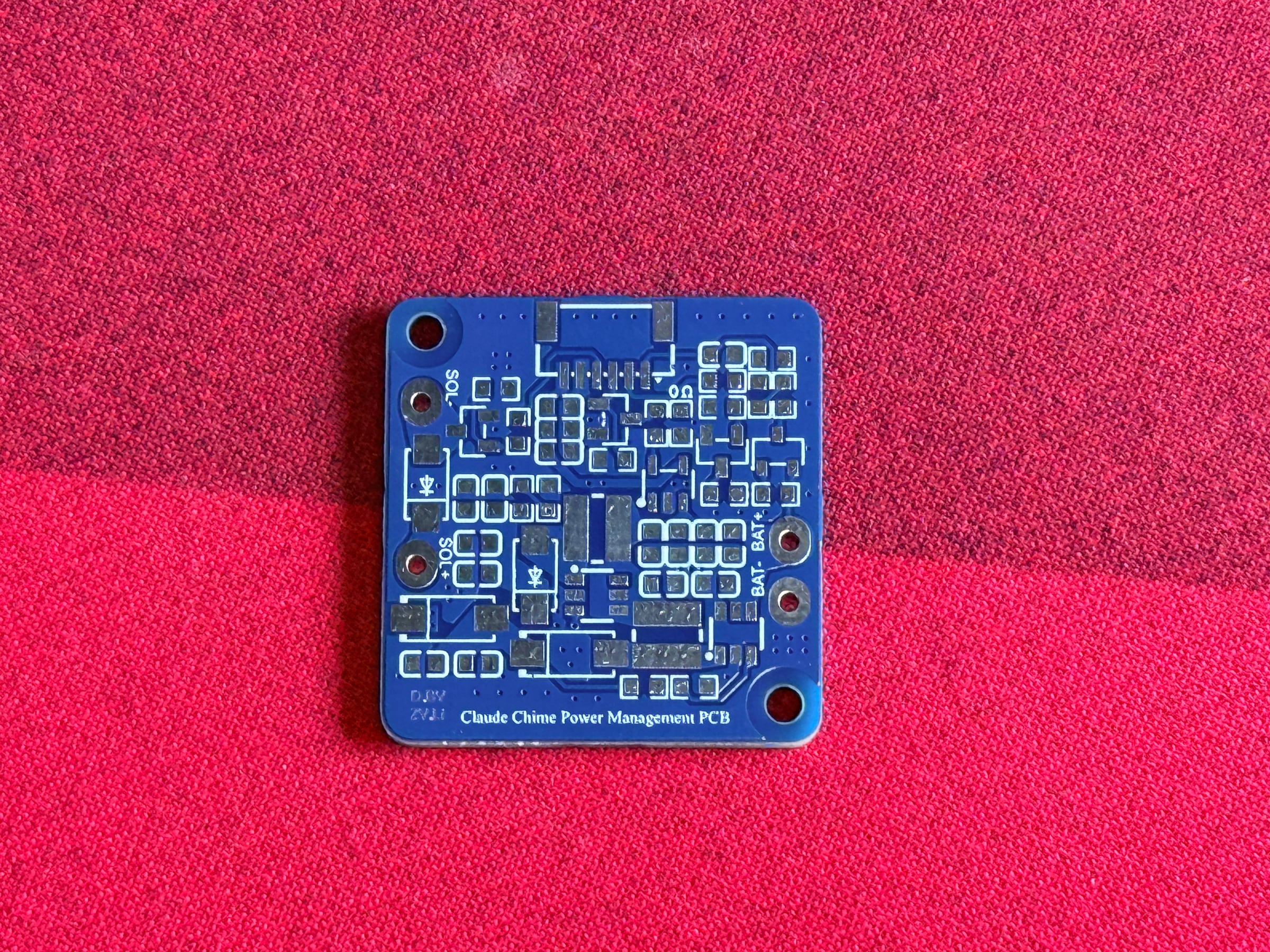
Initial power-up used a 3.8 V bench supply with a 50 mA current limit. The two unloaded boost outputs measured about 5.12 V and 5.08 V, although I can no longer associate each reading with its rail. I confirmed MCP73831 charging current with an ammeter, then observed the battery voltage rising with a multimeter. Alongside the divider check, I repeatedly drove SOL_CTRL using simulated 3.3 V logic levels. The unloaded output kept switching, with no boost-output voltage drop observed during that test.
最初的上电测试用的是 3.8 V、限流 50 mA 的台式电源。两路升压空载输出分别量到约 5.12 V 和 5.08 V,不过现在已经记不清这两个读数各自对应哪一路。我还用电流表确认了 MCP73831 的充电电流,随后用万用表观察到电池电压上升。除了前面提到的分压测试,我也用模拟的 3.3 V 高低电平反复驱动 SOL_CTRL,空载输出能够连续切换,测试时没有观察到升压输出掉压。
The board did not start as expected when I connected the protected battery pack. Before connection, its output measured 4.03 V; on connecting the board, it fell to between 1.49 and 1.57 V. A board that started from a 50 mA-limited supply would not start from this battery, so I kept investigating that difference. The measurements suggest that startup demand may have opened the protection path formed by the DW01A and 8205A. I captured neither the current peak nor the exact protection-state transition, leaving the cause unresolved. The voltage was measured at the pack output; it does not establish that the cell itself fell to the same level.
换成带保护的电池包冷接入,情况就没这么顺利了。接入前,电池包输出端是 4.03 V;一接上板子,就降到了 1.49 至 1.57 V。同一块板明明能从限流 50 mA 的台式电源启动,换成电池却起不来,我也就顺着这个差别继续查。现有测量让我怀疑,上电瞬间的电流需求可能使 DW01A 和 8205A 构成的保护路径断开。但我没有测到电流峰值,也没有记录到确切的保护状态切换,原因还不能定下来。这里量到的是电池包输出端的电压,不能据此认定电芯本身跌到了同样的数值。
The tests that actually made the crab jump happened on the client's side. Neither the real solenoid nor the crab reached my bench, and the client handled the ESP32 firmware. During the project, their firmware engineer reported normal ESP32 communication, ADC battery reading, charge control, repeated solenoid actuation, and complete-device operation. They also said the small power board and six-pin cable saved enclosure space. These were client integration reports, not tests I witnessed.
至于真正带着螃蟹跳起来的测试,是客户那边做的。真实电磁铁和螃蟹都没到过我的测试台,ESP32 固件也由对方负责。客户固件工程师在项目期间的聊天里反馈,ESP32 通信、ADC 电量读取、充电控制、电磁铁反复动作和整机运行都正常,还提到小电源板配合六针排线节省了外壳空间。这些是对方的联调反馈,我没有在场见证。
The boards connect through a six-pin SH1.0 cable carrying ESP_5V_BUS, GND, SOL_CTRL, CHARGE_CTRL, ADC_ENABLE, and ADC_BAT. Before delivery, I documented the interface, the three active-high controls, ADC conversion, charge permissions, and the expected states around Type-C insertion and removal in the software handoff. SOL_CTRL handles the solenoid switch. Getting the power board and core board to work together also required clear instructions for plugging in, unplugging, sensing, and charging.
两块板通过六针 SH1.0 排线连接,接口包含 ESP_5V_BUS、GND、SOL_CTRL、CHARGE_CTRL、ADC_ENABLE 和 ADC_BAT。交付前,我把这些接口以及三路高有效控制、ADC 换算、充电允许条件、Type-C 插拔前后的工作状态写进了软件交接文档。电磁铁的开关由 SOL_CTRL 控制。要让这块电源板和客户的核心板一起工作,插线、拔线、采样、充电时该怎么处理,也都得交代清楚。
Development Notes开发笔记
Debugging records and technical notes tied to the decisions and artifacts on this project page.与这个项目页面中的设计决策和工程材料直接关联的调试记录与技术笔记。
Public Project Files公开项目资料
Uploaded evidence served from the public asset folder. Use the file index to preview documents, source code, media, PDFs, and downloadable artifacts without leaving the page.这里列出已经上传到公开目录的项目证据。可以在左侧索引里选择文件,在右侧直接预览文档、源码、媒体、PDF 和可下载附件。
board-3d-render.png
PNG / 112.9 KB
Related Media相关媒体
Board photos, schematic sheets, videos, and test captures that show this project at specific stages.展示这个项目具体阶段的板卡照片、原理图分页、视频和测试截图。