

2026.09.06
Common-Anode Displays and BCD Decoding共阳数码管与 BCD 译码
Following decimal digit splitting and BCD bit order into active-low LS47 outputs, common-anode LED current paths, segment resistors, and display controls.沿十进制拆位与 BCD 位序,理解 LS47 低有效输出、共阳 LED 电流路径、逐段限流和显示控制。
When the two-digit display reads 17, it looks as though the program has simply moved a number onto the breadboard. Reading the counter program again, I want to follow what happens in between. The Arduino holds a number, the decoders receive two groups of four inputs, and a set of LED segments lights up. Numbers, pin levels, and illuminated segments each have a mapping that needs to make sense.
两位数码管显示 17 时,看上去只是把程序里的数搬到了面包板上。我现在再看这份计数器程序,想把中间的过程拆开弄明白。Arduino 保存的是一个数,送到译码器的是两组四位输入,最后亮起来的却是几段 LED。数字、引脚电平和发光的灯段之间,每一步都有各自的对应关系。
Decimal Digits and BCD十进制数与 BCD
The project report separates the digits with Num % 10 for units and (Num / 10) % 10 for tens. Applying those expressions to 17 gives 7 and 1, which go to separate decoders. BCD represents each decimal digit with four binary bits, so there are two independent digit codes here. The binary representation of the integer 17 is 10001; the two display digits require the BCD groups 0001 0111. Those representations serve different purposes.
作业报告里的拆位方法很直接,Num % 10 取个位,(Num / 10) % 10 取十位。把 17 代进去,得到个位 7、十位 1,再分别送给两颗译码器。BCD 用四个二进制位表示一个十进制数字,所以这里是两个独立的数字编码。若把整数 17 直接按二进制展开,得到的是 10001,和两位显示所需的 0001 0111 不是同一种表示。
The number 1 made me pause when I read the single-digit example. Its array entry is {1, 0, 0, 0}, while I normally expect to see 0001 written down. The pin definitions explain the order. The array follows A, B, C, D, with weights of 1, 2, 4, and 8. Written binary usually puts the most significant bit on the left. Here the first array element goes to A, exactly where it belongs.
我读单个位显示示例时,反而在最简单的数字 1 上停了一下。数组把它写成 {1, 0, 0, 0},而平时写二进制时习惯看到 0001。对照引脚定义就明白了,程序按 A、B、C、D 的顺序存储,权重依次为 1、2、4、8;通常书写的二进制数则把最高位放在左边。数组里的第一个元素先发给 A,顺序完全对得上。
Decimal digit    D C B A    Array order A, B, C, D
      1          0 0 0 1          1, 0, 0, 0
      7          0 1 1 1          1, 1, 1, 0
The example contains sixteen array rows, but % 10 limits the index to 0 through 9 in the loop. Four wires can represent sixteen combinations; one decimal digit uses ten of them. The other six are not automatically hexadecimal characters. TI defines particular patterns for the LS47, whereas the CD4511B blanks inputs above 9. When comparing decoders, I would now check what happens outside the normal digit range as well.
这个示例还有十六行编码,但主循环用 % 10 把索引限制在 0 到 9。四根线能表示十六种组合,十进制的一位只需要其中十种。剩下六种也不能随意当成十六进制字母来显示。TI 的 LS47 说明给它们定义了特定图形,CD4511B 则会将大于 9 的输入消隐。以后换译码器时,除了看 0 到 9,我也会看看越界输入会让输出变成什么。
Active-Low Outputs低有效输出
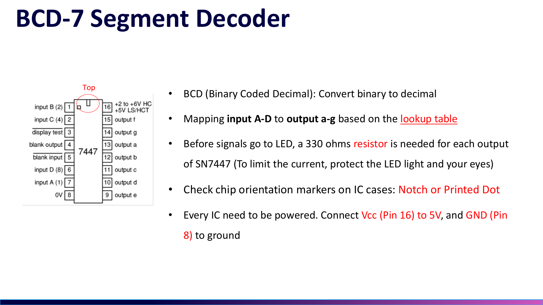
Inputs A through D select the number; outputs a through g correspond to the seven LED segments. With the usual segment labels, 7 lights the top segment a, upper-right b, and lower-right c. The project's SN54LS47 turns those segments on by taking their outputs low. Its datasheet identifies active-low, open-collector outputs for common-anode displays. Following current through the circuit makes that low level easier to interpret.
再往后看,A 到 D 只负责选择数字,译码器的 a 到 g 才对应七段 LED。按常用段位标记,显示 7 要点亮顶部的 a、右上的 b 和右下的 c。对项目里的 SN54LS47 来说,这几个输出变低时,相应的灯段才亮。LS47 数据手册把它的输出标为低有效、开集电极,驱动共阳数码管。这里的低电平要放到电流路径里理解。
In a common-anode display, the segment anodes share a connection to the positive supply. Selecting a segment turns on the corresponding output transistor inside the LS47. Current travels from the supply through that LED and its series resistor, into the driver, and back to ground. Lowering the output voltage forward-biases the LED, causing it to emit light. The relationship between a low output and a lit segment becomes straightforward once I follow that path.
共阳数码管把各段 LED 的阳极连在一起,公共端接到正电源。选中某一段后,LS47 内部的输出晶体管导通,电流从正电源经过该段 LED 和串联限流电阻,流入译码器,再回到地。输出端电压降低,LED 两端反而得到正向电压,于是发光。沿着这条路径看,输出电平与亮灭的关系就顺了。
I also want to look more closely at open-collector operation. When the output transistor turns off, the chip releases the path to ground. The output is then high impedance, with its voltage determined by the external circuit. It does not actively drive the pin up to the supply as a push-pull output would. A segment-off entry in the truth table, the voltage measured at the pin, and the ability to supply current are consequently different things to examine. This makes me pay more attention to why the datasheet calls the part both a decoder and a driver.
开集电极也值得单独看一下。输出晶体管关闭时,芯片松开了这条下拉路径,输出端呈高阻,节点电压由外部电路决定。它不会像普通推挽输出那样主动把引脚推到电源电压。因而,真值表里的不点亮状态、输出引脚上测到的电压,以及能否向外提供电流,要分别理解。我读到这里才更留意数据手册为什么同时写了译码器和驱动器两个身份。
Segment Current and Resistor Selection段电流与限流电阻
The course slide calls for one series resistor per segment output. I want to understand why a single resistor at the display's common pin would not do the same job. With a shared resistor, two LED branches divide the current when displaying 1, and seven do so when displaying 8. Changing the number of lit segments changes the current available to each, making brightness depend on the displayed digit. Individual branch resistors let each segment's current be limited separately.
课件要求每个段输出各串一个限流电阻。我想进一步弄清楚,为什么不在数码管公共端只放一只。假如所有段共用一只电阻,显示 1 时只有两条 LED 支路分电流,显示 8 时变成七条。亮起的段数改变后,每段分到的电流也会改变,亮度就容易随数字变化。电阻分别放在各段支路,才能分别限制各段电流。
For one segment, I would subtract both the LED's forward drop and the driver's on-state low voltage from the supply. Suppose the supply is 5 V, the LED forward drop near the intended current is 2.0 V, and the driver drop is taken as 0.3 V. A target of roughly 5 mA gives (5 − 2.0 − 0.3) / 0.005 = 540 Ω. Using a standard 560 Ω resistor gives about 4.8 mA under the same assumptions. This is an example of choosing a value; the calculation for particular parts needs their electrical parameters.
估算某一段时,我会把 LED 的正向压降和驱动器导通后的低电平电压一起扣掉。假设电源为 5 V,某段 LED 在目标电流附近的正向压降为 2.0 V,驱动输出压降按 0.3 V 计算,希望段电流约为 5 mA,那么电阻约为 (5 − 2.0 − 0.3) / 0.005 = 540 Ω。换成常见的 560 Ω,按同样假设算出约 4.8 mA。这组数值是一个选值例子,具体数码管和芯片还要按各自的电气参数计算。
That gives me a useful way to examine the slide's 330 Ω value. Supply voltage, current, and LED forward voltage belong in the same calculation. Changing the LED while keeping 330 Ω need not preserve the current. When 8 lights all seven segments, their currents also add at the common connection and place a combined load on the supply and driver. I need to consider both each segment and the full digit operating together.
这样看,课件里的 330 Ω 就有了可以继续追问的地方。电阻值要和供电、电流、LED 压降放在一起看;同样用 330 Ω,换一种 LED 后电流未必相同。显示 8 时七段都亮,还要把七路电流加起来,检查公共端、电源和译码器的负担。选电阻既要让每一段合适,也要看整位显示一起亮时怎样工作。
Decoder and Display Compatibility译码器与数码管的匹配
The CD4511B used in the course simulation makes the difference concrete. It supplies segment current for common-cathode LEDs. An active segment output goes high, sending current through the LED and its limiting resistor to the common cathode and ground. The two chips therefore require different common connections and active output levels for the same input digit. Both turn BCD into a seven-segment pattern, but the LED connections have to match the output structure.
再对照课件仿真里的 CD4511B,差别就很具体了。它为共阴 LED 提供段驱动电流,选中的段输出高电平,电流从输出端经过 LED 和限流电阻流向公共阴极,再回到地。同样送入一个数字,两种芯片要求的公共端接法和段输出有效电平不同。它们都能把 BCD 变成七段图形,连接 LED 的方式却要随输出结构一起选。
The test and blanking pins need checking alongside the four data inputs. The LS47 controls include lamp test, blanking, and zero suppression, all of which affect what appears on the display. A correct value on A through D can still be hidden by those controls. For a single-digit check, I would first establish normal decoding conditions from the truth table, then hold the inputs at 1, 7, and 8 in turn. That sequence checks the two right-hand segments, adds the top segment, then exercises all seven.
四位输入确认以后,还要检查测试和消隐脚。LS47 的控制说明列有灯测试、消隐和零消隐功能,这些控制会参与决定显示状态。如果只查 A 到 D,忽略了这些脚的状态,就可能遇到输入数字正确、显示仍然被关闭的情况。调试单个位时,我会先按真值表设好正常译码条件,再固定送入 1、7 和 8,逐步检查右侧两段、顶部一段和全部七段。
An incorrect digit calls for checking BCD bit order and the decoder's control inputs; a missing segment can be investigated along its LED branch. Those are different starting points. Once I can connect the visible error to the relevant pins and expected current path, I have a concrete way to investigate it.
缺一段和整位显示成另一个数字,可以从不同的地方查起。前者沿对应的 LED 支路检查,后者先核对 BCD 位序和译码器的控制条件。显示错了什么、哪些引脚控制着它、电流应该从哪里流过,这几件事能对上,调试就有了具体的方向。