Note 02 of 04: 笔记 02 / 04:dBm, Vpp and the IF Output LeveldBm、Vpp 与中频输出电平
What dBm measures and why RF work uses it, then the AD831 mixer board's IF output recomputed from the signal source to the scope: why 150 mVpp over 100 Ω was the wrong division, what a 1 MΩ scope input actually reads, and where the link budget's −6 dB really belongs.dBm 是什么、射频里为什么都用它,再把 AD831 混频器板的中频输出从信号源一路推到示波器:150 mVpp 为什么不该除以 100 Ω,1 MΩ 输入的示波器读到的是什么,链路预算里那个 −6 dB 实际该记在哪。
Partway through the demo video there is a calculation: the 150 mVpp IF on the scope corresponds to about −15.5 dBm, which agrees well with a link budget of −19 dBm − 6 dB + 10 dB = −15 dBm. The reasoning went like this. A 50 Ω resistor, R3, sits in series after the chip's OUT pin; the scope input was taken to be 50 Ω; so the chip sees 100 Ω in total, and 150 mVpp gets converted to power over 100 Ω. At the time, the two numbers simply matched.
演示视频里有一段算账:示波器上量到 150 mVpp 的中频,对应约 −15.5 dBm,和 −19 dBm − 6 dB + 10 dB = −15 dBm 的链路预算很吻合。算法是这样的:芯片 OUT 后面串了一个 50 Ω 的 R3,示波器入口当成 50 Ω,芯片看出去一共 100 Ω,于是拿 150 mVpp 对 100 Ω 算功率。当时这两个数就这么对上了。
What dBm MeasuresdBm 的定义
dBm is power in decibels relative to 1 mW: P(dBm) = 10 log₁₀(P / 1 mW). 0 dBm is 1 mW, +10 dBm is 10 mW and −30 dBm is 1 µW. Almost everything in RF is labelled this way: the tinySA Ultra screen reads −19.0 dBm, the SG6-A is set to −10 dBm, and the intercept and compression points in the AD831 datasheet are all in dBm.
dBm 是以 1 mW 为参考的功率分贝数,P(dBm) = 10 lg(P / 1 mW)。0 dBm 是 1 mW,+10 dBm 是 10 mW,−30 dBm 是 1 µW。射频里几乎所有东西都用它来标:tinySA Ultra 屏幕上写 −19.0 dBm,SG6-A 设成 −10 dBm,AD831 手册里的截点、压缩点也都是 dBm。
The convenience is practical. Multiplication becomes addition: gains and losses along a chain are a string of ratios to multiply, and in decibels they simply add, which is how a link budget gets written line by line. It also compresses huge ranges; wanted signals and noise in RF are often ten orders of magnitude apart, which in dBm is a span of about 100 dB. And there's a reason tied to impedance. RF ports, cables and instruments almost all standardise on 50 Ω, and along a matched chain power is conserved while voltage changes with impedance, so power becomes the common currency. Rohde & Schwarz's dB or not dB application note walks through all of these conversions.
用 dBm 方便在几处。乘除变加减:一条链路上的增益和损耗原本是一串倍数相乘,换成分贝以后直接相加,链路预算就是这么一行一行加出来的。它还能装下很大的范围,射频里有用信号和噪声动辄差上十个数量级,写成 dBm 也就是一百 dB 的跨度。还有一层原因和阻抗有关,射频系统的端口、电缆、仪器几乎都统一在 50 Ω 上,在匹配好的链路里,功率沿途守恒,电压却随阻抗变化,于是功率成了通用的量。Rohde & Schwarz 的 dB or not dB 应用笔记把这些换算都梳理了一遍。
Because dBm is power, converting from a voltage needs the resistance that voltage sits across. For a sine wave, P = (Vpp / 2√2)² / R. 0 dBm across 50 Ω is 223.6 mV RMS, or 632 mVpp. The same 150 mVpp is −12.5 dBm across 50 Ω and −15.5 dBm across 100 Ω, a full 3 dB apart.
正因为 dBm 是功率,从电压换过去时必须知道电压落在多大的电阻上。正弦波 P = (Vpp / 2√2)² / R。0 dBm 加在 50 Ω 上是 223.6 mV 有效值,也就是 632 mVpp。同样的 150 mVpp,落在 50 Ω 上是 −12.5 dBm,落在 100 Ω 上是 −15.5 dBm,差了整整 3 dB。
The Original Calculation当时那笔账
Even granting the original assumption of a 50 Ω scope input, the 150 mVpp is the voltage across that input. It describes the power the scope absorbs and should be divided by 50 Ω, giving −12.5 dBm. Dividing by 100 Ω treats the scope-input voltage as if it appeared across the whole 100 Ω, mixing up two different places in the circuit.
按当时的想法,就算示波器入口真是 50 Ω,那 150 mVpp 也是示波器入口两端的电压,它对应的是示波器吃到的功率,应该拿 50 Ω 去算,得到 −12.5 dBm。拿它除以 100 Ω,等于把示波器入口的电压当成了加在整个 100 Ω 上的电压,两个位置混在了一起。
Scope Input Impedance示波器的输入阻抗
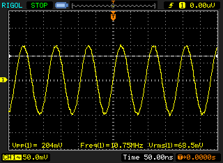
Digging further, the 50 Ω premise doesn't hold either. The settings file the RIGOL exported alongside its capture states the channel input impedance plainly as 1M Ohm. In the video, both scopes are connected through plain SMA-to-BNC adapters with no 50 Ω terminator in between. With a 1 MΩ input, almost no current flows through R3, so the scope reads the output amplifier's open-circuit voltage, and the load the chip sees is around a million ohms.
再往下查,连那个 50 Ω 的前提也不成立。RIGOL 存图时一并导出的设置文件里写得很清楚,通道输入阻抗是 1M Ohm。视频里两台示波器都是用 SMA 转 BNC 的转接头直接插上去的,中间没有 50 Ω 终端。示波器入口是 1 MΩ 的话,R3 上几乎没有电流,示波器读到的就是输出放大器的开路电压,芯片看出去的负载也就成了一百万欧左右。
From Source to Scope从信号源推到示波器
With that premise, the chain can be worked from the start. The tinySA Ultra's −19 dBm is the power it delivers into a 50 Ω load, which is 71 mVpp across a matched load. The input network looks like about 47.6 − j11.1 Ω from the SMA (derived in Lumped Matching and Trace Impedance), so the voltage reaching RFP is about 0.94 times the matched voltage, around 67 mVpp. The AD831's mixer core has nominal unity gain in the datasheet, 0 dB from RF voltage to IF voltage. The output amplifier after it is set by R1 = 51 Ω and R2 = 110 Ω to (51 + 110) / 51 ≈ 3.16 times, or 10 dB. The open-circuit voltage at OUT is therefore about 67 × 3.16 ≈ 210 mVpp.
换成这个前提,从头推一遍。tinySA Ultra 的 −19 dBm 是它对 50 Ω 负载给出的功率,落在匹配负载上是 71 mVpp。输入网络从 SMA 看进去约 47.6 − j11.1 Ω(推导在集总匹配与走线特性阻抗里),送到 RFP 上的电压约为匹配电压的 0.94 倍,也就是 67 mVpp 左右。AD831 的混频核心在数据手册里是名义上的单位增益,RF 电压到中频电压是 0 dB;后面的输出放大器由 R1 = 51 Ω、R2 = 110 Ω 定成 (51 + 110) / 51 ≈ 3.16 倍,也就是 10 dB。OUT 脚的开路电压于是约为 67 × 3.16 ≈ 210 mVpp。
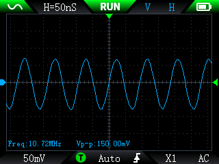
The RIGOL capture reads 204 mVpp at 10.75 MHz, only about 0.3 dB from the predicted 210 mVpp. The handheld scope in the video read 150 mVpp, a fair bit lower than the RIGOL, so the calculation here goes by the RIGOL capture.
RIGOL 那次存下的读数是 204 mVpp、10.75 MHz,和推出来的 210 mVpp 只差 0.3 dB 左右。视频里的手持示波器读到的是 150 mVpp,比 RIGOL 低一截,这里的推算以 RIGOL 这次为准。
If the IF output drove a real 50 Ω load, say a tinySA Ultra used as a spectrum analyzer, R3 and the load would split the voltage in half, leaving about 102 mVpp, or −15.8 dBm. Written as a power budget: −19 dBm in, a well-matched input with almost no loss, +10 dB from the output amplifier, then −6 dB from R3 dividing against the 50 Ω load, for roughly −15 dBm. The old budget had a −6 dB too, but it was booked at the input. The 6 dB is actually spent at the output, in R3. Booked at the wrong end, that −6 dB happened to make the total come out right.
如果中频端接的是真正的 50 Ω 负载,比如把 tinySA Ultra 当频谱仪接上去,R3 和负载对半分压,负载上只剩一半,约 102 mVpp,换算成功率是 −15.8 dBm。拿功率来写链路预算,就是 −19 dBm 进来,输入端匹配良好、几乎没有损失,输出放大器加 10 dB,R3 和 50 Ω 负载分压再减 6 dB,得到约 −15 dBm。当时那张预算表里也有一个 −6 dB,只是记在了输入端;实际吃掉这 6 dB 的是输出端的 R3。放错位置的 −6 dB,正好把总数凑对了。
The 150 mVpp reading was trustworthy all along; the resistor it got divided by was the wrong one. dBm is power, and power only has a value once it lands on some resistance. Given a Vpp, first pin down which two points it was measured between and what impedance it was looking into, and the decibels that follow will come out right.
150 mVpp 这个读数一直都可信,换算时用错的是电阻。dBm 说的是功率,功率总要落在某个电阻上才有数,拿到一个 Vpp,先弄清它是哪两点之间、对着多大的阻抗量出来的,后面的分贝才算得明白。