Project 04 of 11: 项目 04 / 11:AD831 Active Mixer BoardAD831 有源混频器板
EEE307 coursework at XJTLU: an RF mixer board built around ADI's AD831 that turns a 120 MHz signal and a 130.7 MHz LO into a 10.7 MHz IF. It started from a contest-guide reference circuit and went through four PCB versions in five weeks, mostly reworking the input high-pass and the IF output.西浦 EEE307 课程作业。用亚德诺的 AD831 做了一块射频混频器板,把 120 MHz 的 RF 和 130.7 MHz 的本振混成 10.7 MHz 中频。从电赛备赛指南里的参考电路起步,五个星期改了四版 PCB,主要在折腾输入端的高通和中频输出端。
Coursework and Reference Circuit选题与参考电路
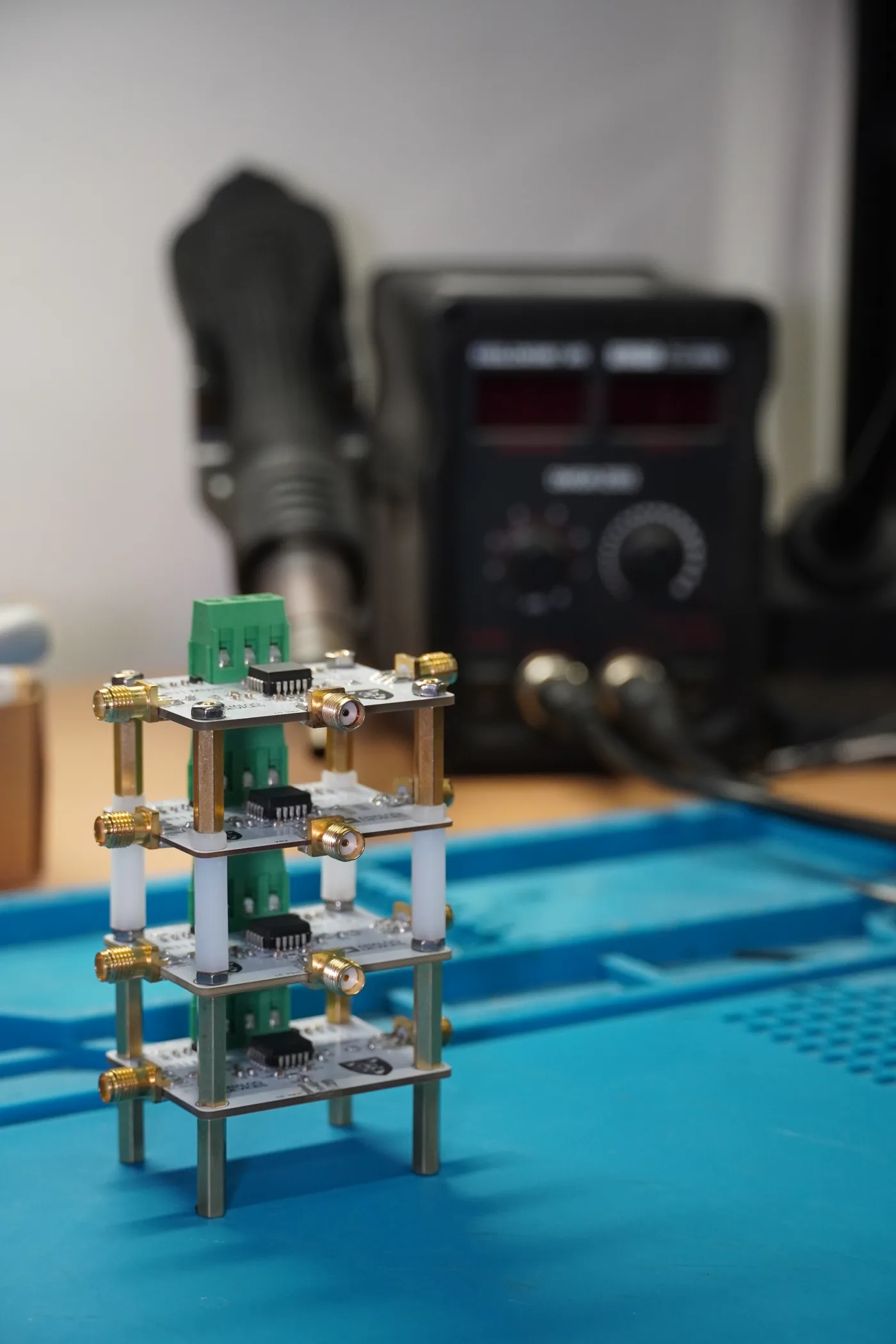
Four white AD831 mixer boards sit side by side on the desk. The front silkscreens run from V1.0 to V4.0, and the JLCPCB batch codes on the back read 251020, 251107, 251115 and 251124: five weeks from the first order to the fourth. They came out of the circuit-construction coursework for EEE307 Electronics for Communications at XJTLU, worth 20% of the module. Pairs picked any communications circuit, built it, tested it, and explained it in a video of three minutes or less. I worked with my roommate Zichen.
桌上并排摆着四块白色的 AD831 混频器板,正面丝印从 V1.0 排到 V4.0,背面嘉立创的批次号分别是 251020、251107、251115、251124。从第一版下单到第四版,前后五个星期。这是西浦 EEE307 Electronics for Communications 的电路制作作业,占这门课总评的 20%,两人一组,自己挑一个和通信有关的电路,做出来、测出来,再拍一段三分钟以内的视频讲清楚。我和舍友 Zichen 一组。
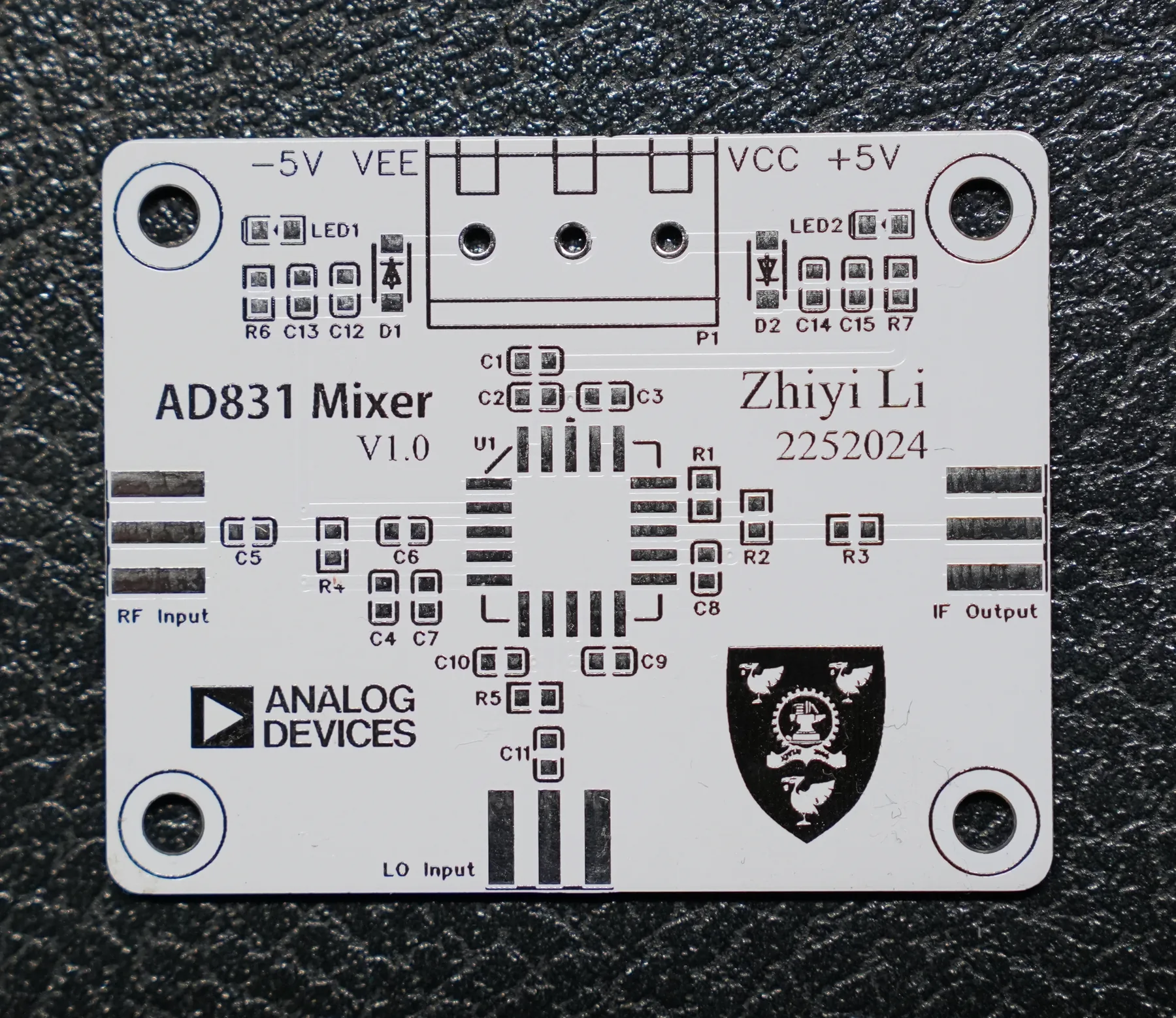
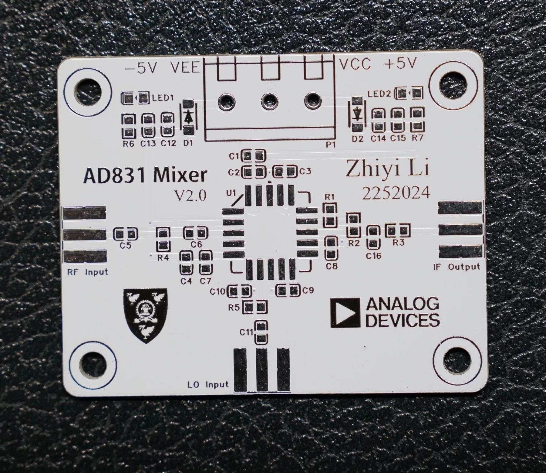
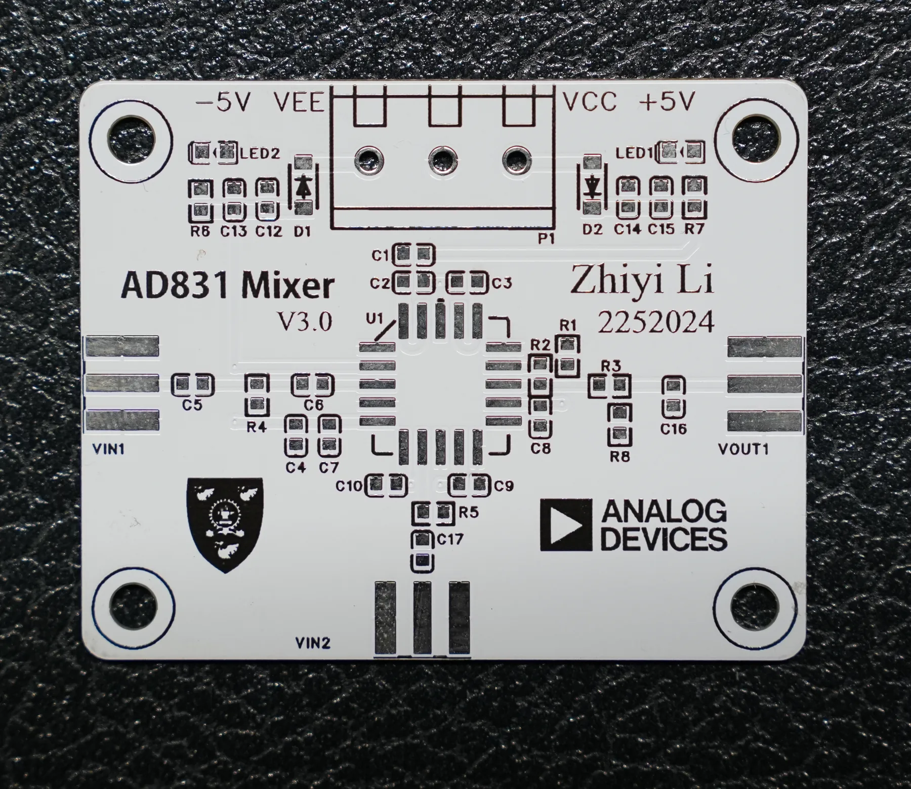
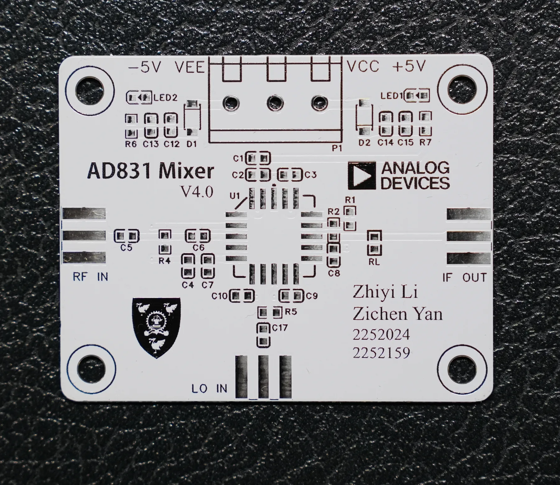
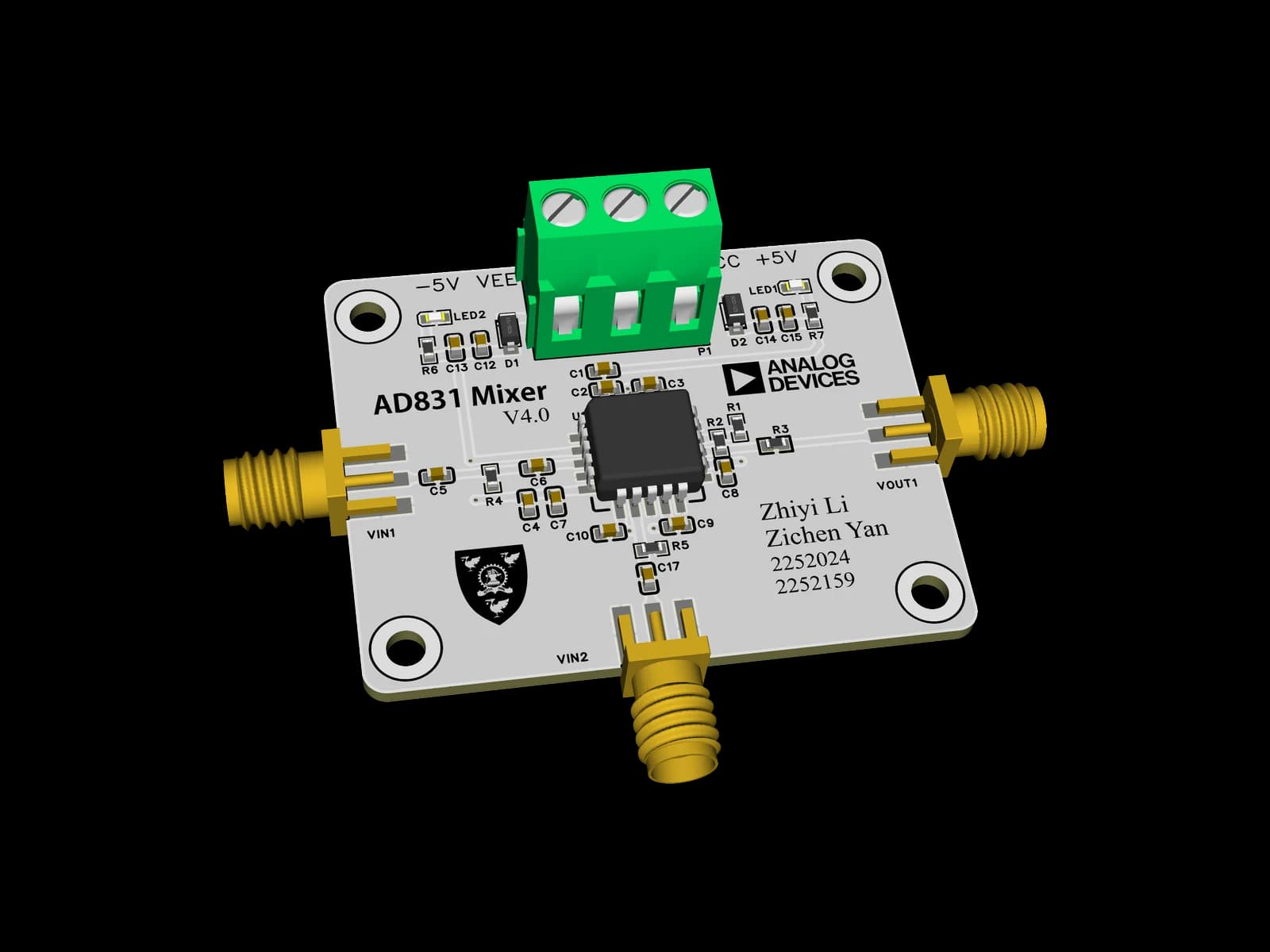
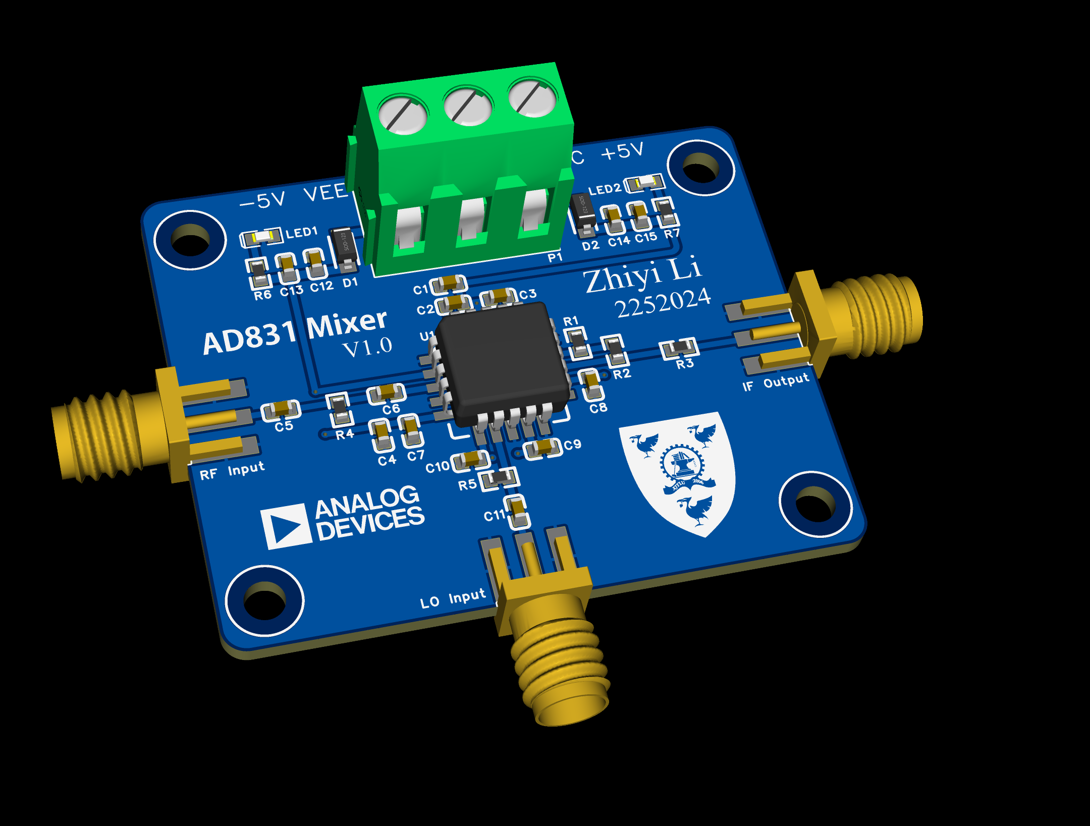
The module started with how resistors, capacitors and inductors behave at high frequency, then worked through LC filters, low-noise amplifiers, mixers, oscillators and phase-locked loops. The bar for the coursework was generous, since a passive filter counted, so most classmates built high-pass and low-pass filters on breadboards from colour-banded resistors and through-hole capacitors. Hardly anyone built a mixer. I wanted something with more weight than a filter and performance I could rely on. Honestly, there was some laziness in it too: that semester I was also running my final-year project and working part-time at Juanyun, so I took ADI's ready-made AD831 mixer chip, spent my effort on the board, and used it to learn how an RF signal should travel from an SMA connector to a chip pin. I had just finished the national electronic design contest in summer 2025 and still had its LCEDA-based preparation guide. Chapter 8 happened to be an AD831 low-distortion mixer reference circuit, and V1 was drawn straight from it.
这门课从高频下的电阻、电容、电感讲起,一路讲到 LC 滤波器、低噪声放大器、混频器、振荡器和锁相环。作业门槛放得很宽,搭一个无源滤波器也算数,所以大部分同学是在面包板上用色环电阻和插件电容搭高通、低通,做混频器的很少。我想做个比滤波器有分量、性能又有保证的东西。说实话也有偷懒的成分:那学期同时在做毕设,还在卷云做兼职,时间实在不多,于是直接用了亚德诺的现成混频芯片 AD831,把力气花在板子上,顺便学一学射频信号从 SMA 头走到芯片管脚这一路该怎么处理。2025 年暑假刚打完电赛,手边还有那本基于立创 EDA 的电赛备赛指南,第 8 章正好是一个 AD831 低失真混频器的参考电路,V1 就是照着它画的。
V1 was ordered on 20 October. The mixer lecture was on 31 October. The board arrived before the lesson did, which is a slightly cheeky head start.
V1 在 10 月 20 日下单,课上讲混频器那一讲排在 10 月 31 日。板子比课先到,多少有点抢跑。
Four PCB Revisions四版 PCB 的改动
Once V1 was soldered, I started checking it against what the lectures taught. Capacitors and inductors stop being pure capacitors and inductors at high frequency; each carries ESR and ESL, and you have to account for the capacitive and inductive reactance so the imaginary parts cancel and the real parts line up, or the signal reflects at the interface. That was the only kind of impedance matching in my head at the time. Working through it that way, I concluded the reference circuit would reflect as soldered, with neither end matched, so I started alternating between the input and the output. That went on for four versions.
V1 焊好以后,我开始拿课上讲的那套去对它。老师讲过,电容、电感到了高频都不再是纯粹的电容、电感,各自带着 ESR 和 ESL,要把容抗、感抗都算进去,让虚部抵消、实部对上,信号才不会在接口处反射回去。当时我脑子里的阻抗匹配就是这一种。照这个思路去算,我觉得参考电路直接焊上会有反射,两头的阻抗都对不上,于是输入端和输出端开始轮流改,一改就改了四版。
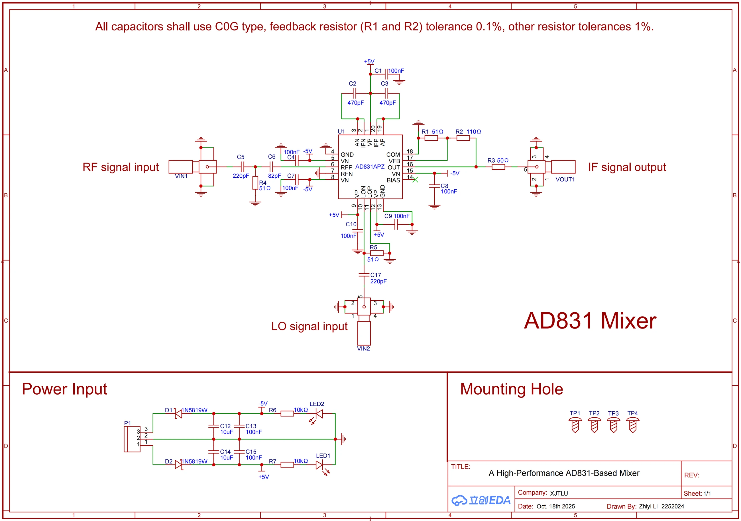
The IF end was the first to change. The reference circuit hung 82 pF on each of the chip's two IF current outputs, forming a first-order low-pass with the roughly 14 Ω internal load. Only after reading the datasheet did I find where 82 pF came from: an example for a 70 MHz IF, with the corner placed an octave above it at 140 MHz. My IF was 10.7 MHz. Copied as-is, that filter would let most of the 130.7 MHz LO leakage and the 250.7 MHz sum product straight through. The final version uses 470 pF, which puts the corner around 24.2 MHz: 10.7 MHz passes and everything above it gets pushed down.
先改的是中频那一头。参考电路在芯片的两个中频电流输出脚上各挂了一颗 82 pF,和芯片内部约 14 Ω 的负载电阻组成一阶低通。翻数据手册才知道,82 pF 出自手册里一段 70 MHz 中频的示例,转折点放在中频往上一个倍频程,也就是 140 MHz。可我的中频只有 10.7 MHz,照搬过来,130.7 MHz 的本振泄漏和 250.7 MHz 的和频基本都能漏过去。最终版把这两颗换成 470 pF,转折频率落到 24.2 MHz 左右,10.7 MHz 照样通过,再往上的成分被压了下去。
The RF input kept the same structure through all four versions: a series capacitor from the SMA, a 51 Ω shunt to ground, then another series capacitor into RFP. Only the capacitor values changed. V1 used 10 nF, whose reactance at 120 MHz is around a tenth of an ohm, so it was effectively a wire that only blocked DC. The final version uses 220 pF and 82 pF. Each one forms a high-pass with the source resistance or the 51 Ω, with corners near 14.5 MHz and 38 MHz, so low-frequency interference stays out while the source still sees close to 50 Ω. The LO path keeps a single coupling capacitor and its 51 Ω, with no second stage, to leave the LO a wider usable frequency range.
RF 输入这一路,四版的结构一直没变:SMA 进来先串一颗电容,再对地并一个 51 Ω,然后串一颗电容进 RFP。变的是电容值。V1 用的是 10 nF,在 120 MHz 下容抗只有零点一欧量级,几乎就是一根导线,只管隔直。最终版换成 220 pF 和 82 pF,两颗电容分别和信号源内阻、51 Ω 组成两级高通,转折频率大约在 14.5 MHz 和 38 MHz,低频干扰被挡在外面,信号源看进来仍然接近 50 Ω。本振那一路只留一颗耦合电容加 51 Ω,不再多加一级,好让本振可用的频率范围宽一些。
The IF output changed the most. I was convinced the oscilloscope input was 50 Ω, so I wanted the chip's output to look like 50 Ω as well. V2 added a shunt capacitor, C16, on the output line. V3 became a series R3 followed by a shunt R8 and C16, which mixed attenuation, matching and filtering into one network. V4 cleared all of that away and left a single RL footprint so I could solder different values and try them. The final choice was R3 = 50 Ω. The feedback resistor R2 went from 100 Ω to a 0.1% 110 Ω part, which with the 51 Ω R1 sets the output amplifier's gain to 10 dB.
改得最多的是中频输出端。我当时一直以为示波器的输入是 50 Ω,所以想让芯片输出端看出去也是 50 Ω。V2 在输出线上加了一颗对地电容 C16;V3 变成串联电阻 R3 加上对地的 R8 和 C16,像是把衰减、匹配和滤波揉在了一起;到 V4 干脆全部收掉,只留一个 RL 焊盘,准备焊不同阻值的电阻上去试。最后定下来的是 R3 = 50 Ω。反馈电阻 R2 从 100 Ω 换成 0.1% 精度的 110 Ω,和 51 Ω 的 R1 一起把输出放大器的增益定在 10 dB。
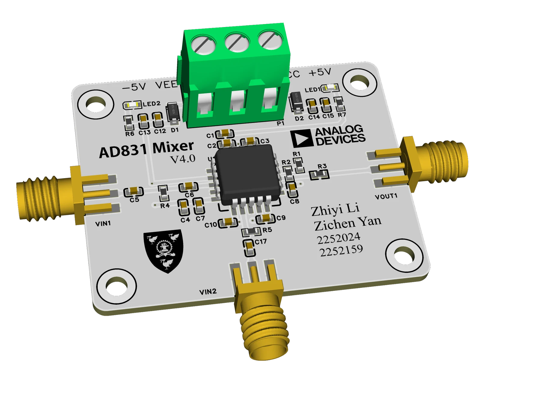
Routing never crossed my mind as an impedance question. I never worked out a 50 Ω trace width from the stack-up; I just kept the RF, LO and IF traces short, left the ground solid, and put the decoupling capacitors right against the supply pins. The kind of matching where differential pairs are drawn at 90 Ω and RF lines at 50 Ω came to me later. How it relates to the lecture kind, where components cancel the imaginary part, is worked through again in Lumped Matching and Trace Impedance.
走线这件事,当时完全没往阻抗上想。我没有按叠层算过 50 Ω 线宽,只是尽量把 RF、本振、中频三条线画短,地铺完整,去耦电容贴着电源脚放。画差分线要算 90 Ω、画射频线要算 50 Ω 的那种阻抗匹配,是后来才接触到的。它和课上那种靠元件抵消虚部的匹配是什么关系,我在集总匹配与走线特性阻抗里重新理了一遍。
Bench Tests and Results测试与结果
Most of the debugging happened at the studio in the sunken plaza, on a battery box, with handheld instruments only. A tinySA Ultra served as the signal source for a 120 MHz, −19 dBm RF input, an SG6-A supplied the 130.7 MHz, −10 dBm LO, and an ALIENTEK DS100 watched the IF. The difference of the two is 10.7 MHz, the most common IF in FM radio. The mixing table in the datasheet uses the very same set of conditions: RF 120 MHz, LO 130.7 MHz, ±5 V.
调试大多在下沉广场的工作室里做,电池盒供电,仪器全是手持的:tinySA Ultra 当信号源,出 120 MHz、−19 dBm 的 RF;SG6-A 出 130.7 MHz、−10 dBm 的本振;正点原子 DS100 看中频。两个频率一减,差频是 10.7 MHz,正好是调频收音机里最常用的那个中频。数据手册里那张混频表,用的也是 RF 120 MHz、本振 130.7 MHz、±5 V 这一组条件。
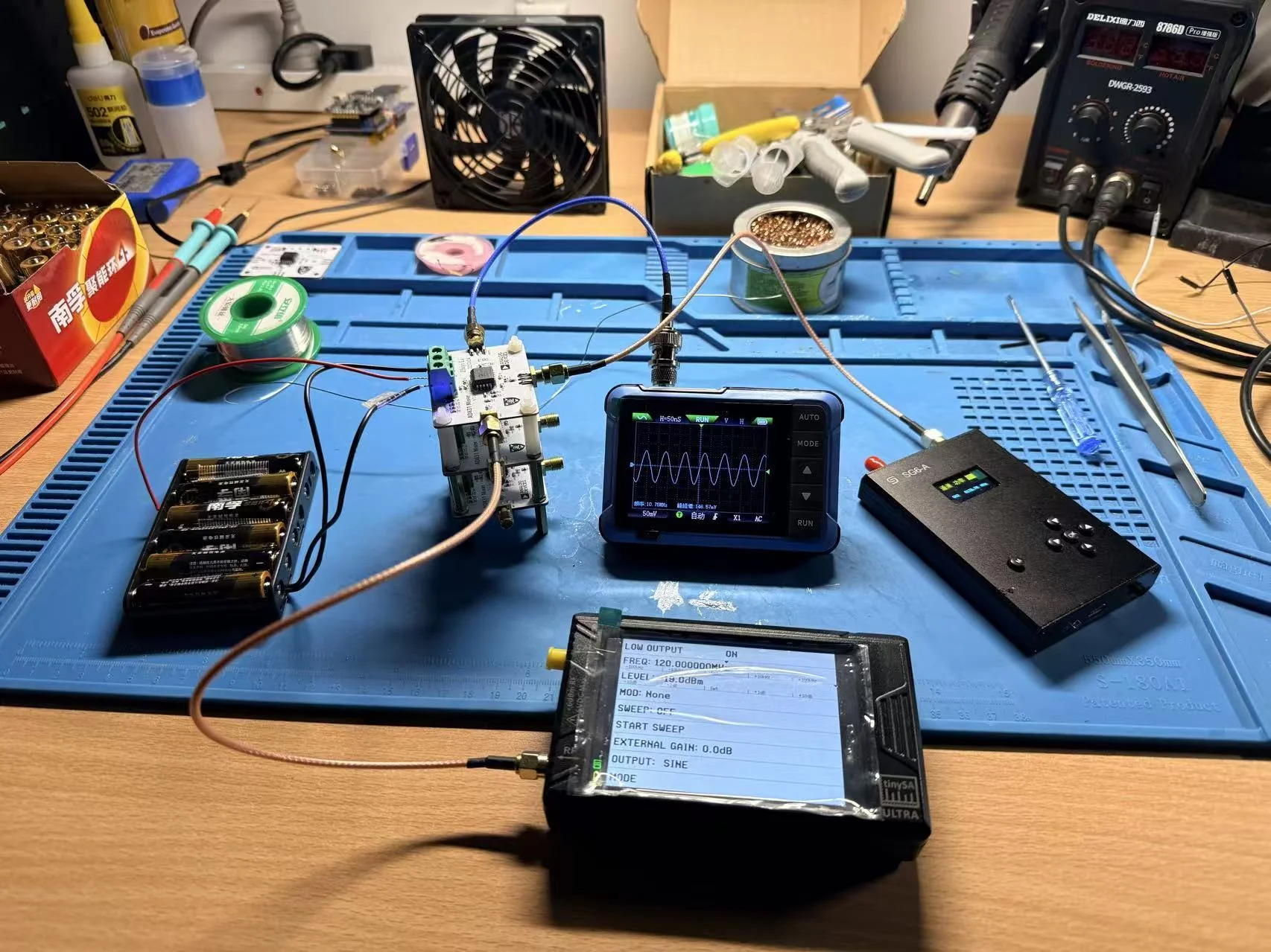
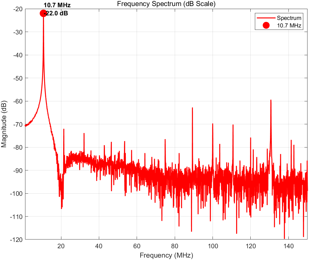
The final captures and the video were done in the lab. The ±5 V came from a Lihe LK3303D dual supply instead, and both current readouts sat around 0.09 A, close to the roughly 100 mA quiescent current the datasheet gives at ±5 V. On the handheld scope the IF output was a clean 10.72 MHz sine at 150 mVpp. Turning off either the RF or the LO made the 10.7 MHz tone vanish at once, so it really was a mixing product. An FFT of the raw waveform saved from the lab's RIGOL scope puts the 130.7 MHz LO leakage a little over 30 dB below the 10.7 MHz peak.
最终的存图和视频是在实验室拍的。±5 V 改由 Lihe LK3303D 双路电源提供,两路电流读数都停在 0.09 A 左右,和手册里 ±5 V 下一百毫安上下的静态电流差不多。手持示波器上,中频输出是一条干净的 10.72 MHz 正弦,峰峰值 150 mVpp。把 RF 或本振任意关掉一路,10.7 MHz 立刻消失,说明这个信号确实是混出来的。拿实验室 RIGOL 示波器存下的原始波形做 FFT,10.7 MHz 主峰旁边,130.7 MHz 的本振泄漏比它低三十多 dB。
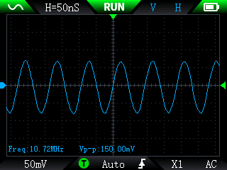
At the time I converted the 150 mVpp to power over 100 Ω: 50 Ω in series at the output plus what I took to be a 50 Ω scope input. That gave about −15.5 dBm, which lined up neatly with a link budget of −19 dBm minus 6 dB plus 10 dB. Only later did it become clear that the scope input was actually 1 MΩ, which calls for a different calculation. The full derivation is in dBm, Vpp and the IF Output Level.
这 150 mVpp 换成功率是多少,当时是按 100 Ω 算的:输出端串了 50 Ω,示波器入口也当成 50 Ω,加起来 100 Ω,算出约 −15.5 dBm,和 −19 dBm 减 6 dB 再加 10 dB 的链路预算刚好对上。后来才弄清示波器其实是 1 MΩ 输入,这笔账得换个算法,完整的推导在 dBm、Vpp 与中频输出电平。
Demo Video and Defense演示视频与答辩
We recorded the video together. Beforehand I walked Zichen through the principle: what the block diagram inside the chip looks like, and why two signals come out of it mixed the way they do. Once that made sense, we split the narration between us and cut it into a demo video just under three minutes long.
视频是两个人一起录的。录之前,我先把原理给 Zichen 讲了一遍:芯片内部的框图长什么样,两个信号为什么混出来会是这个样子。讲明白以后两人分段讲解,剪成一段不到三分钟的演示视频。
At the in-person demonstration, the lecturer opened by saying the slides I had made were well done. That was nice to hear, since I was quite pleased with them myself. Then he pointed at the circuit on them and asked Zichen why the chip needs plus and minus 5 V. He answered it: the two supplies bias the transistors inside the chip so they operate in the right region. My question was different. For a mixer, which two specifications matter most? The datasheet lists a long row of parameters, and I couldn't tell which two he wanted. I gave two from the noise side, saw he didn't look quite satisfied, and added two more from the linearity side. Noise figure and the third-order intercept were among them. He smiled and said that was fine, and that was the defense. Why those two come first is written up in Mixer Performance Metrics.
现场答辩时,老师先夸了一句我做的那份 PPT 不错。这话听着挺受用,那几页我自己也觉得做得挺好。接着他指着 PPT 上的电路问 Zichen,这颗芯片为什么要接正负 5 V。他答上来了:这两路电源给芯片里的晶体管提供合适的偏置,让它们工作在该在的区域。问我的是另一个问题:对一个混频器来说,最重要的两个指标是什么?手册里列的参数一大串,我一时拿不准老师想听哪两个,先从噪声那边答了两个,看老师表情不太满意,又从线性度那边补了两个,噪声系数和三阶交调截点都在里面。老师笑着说没问题,答辩就这么过了。这两个指标为什么排在最前面,写在混频器的性能指标。
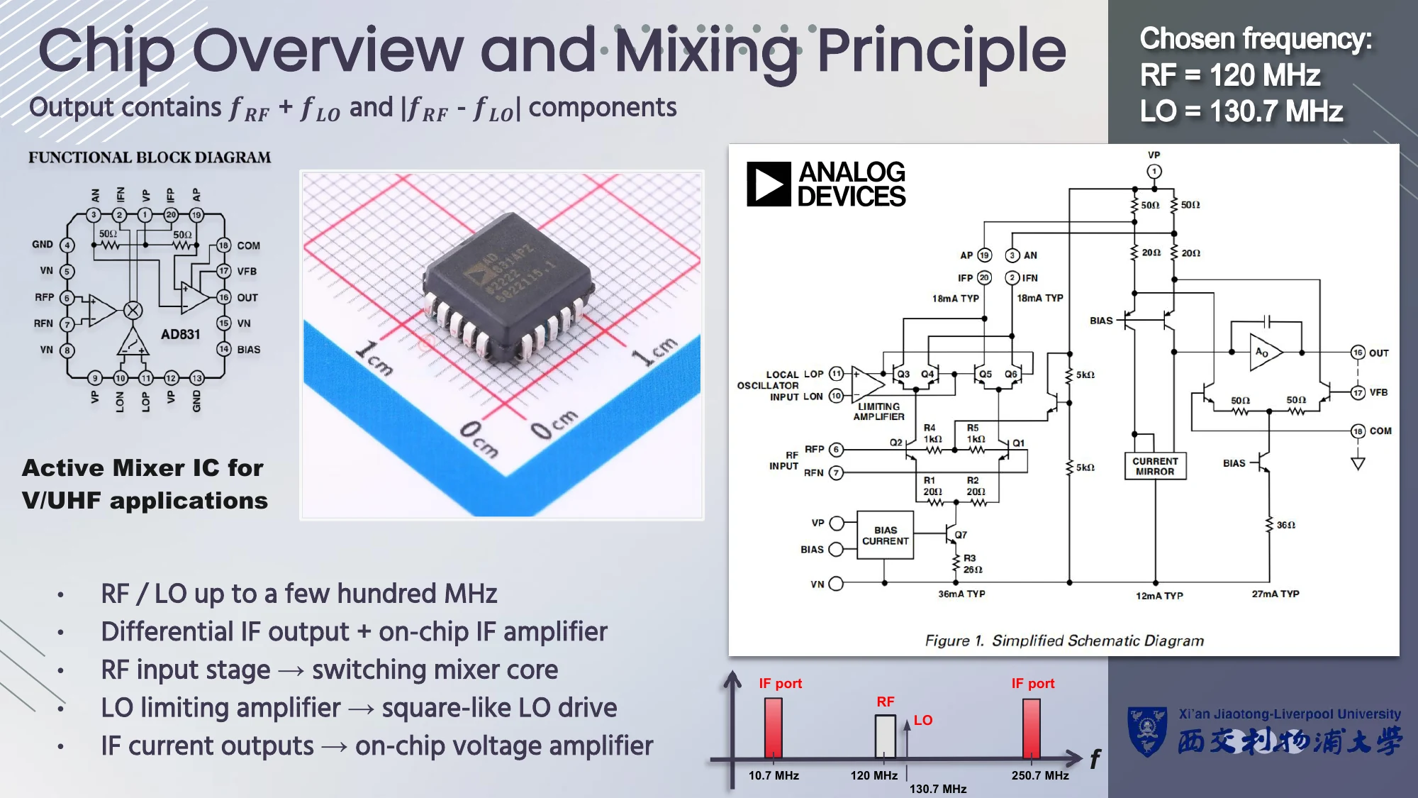
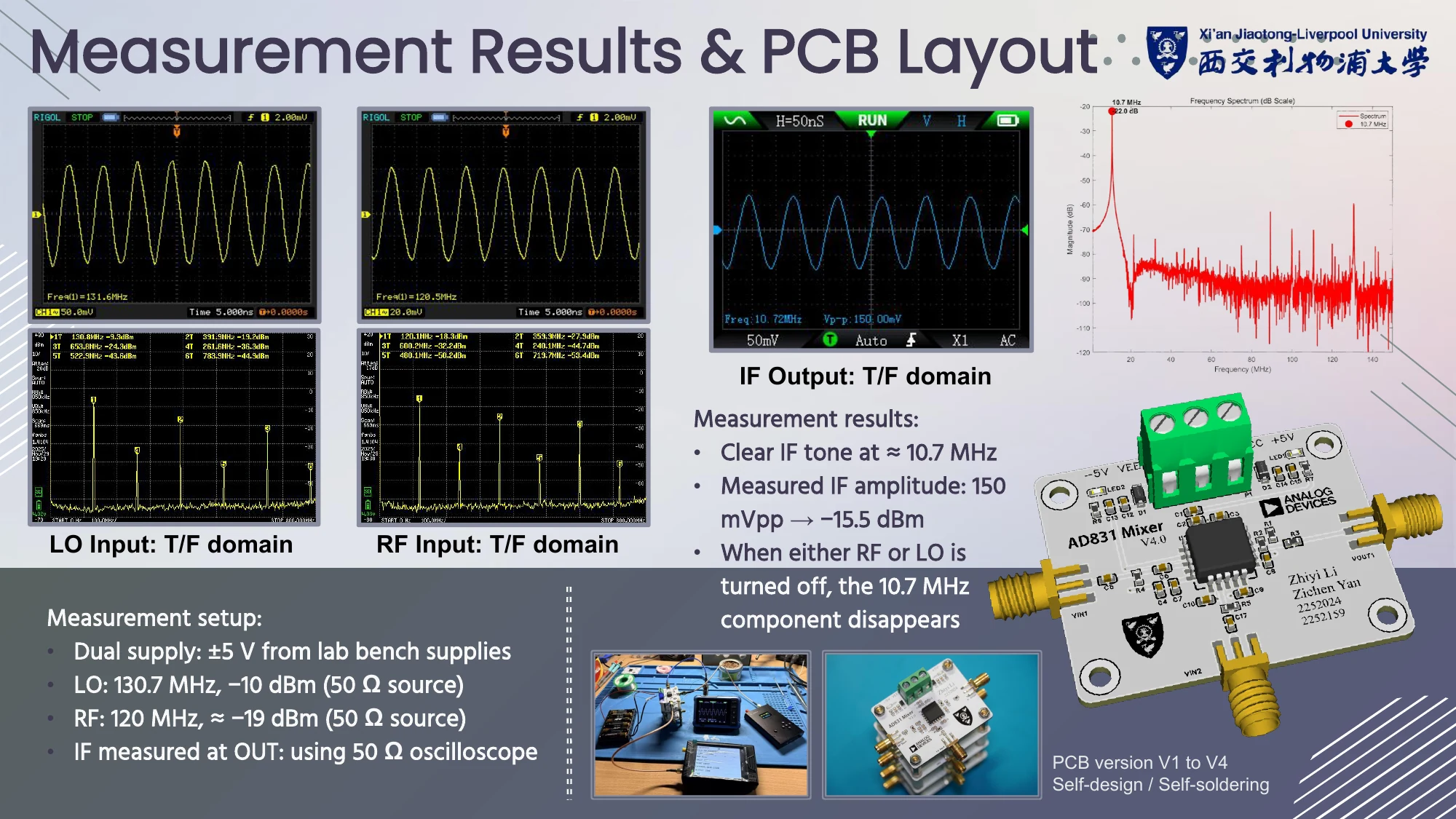
The coursework came back at 78, an A on the transcript. This lecturer marked fairly hard, and as I remember most people landed in the low sixties. Getting that mark on the back of a ready-made chip leaves me a little sheepish. Luckily I've graduated, and nobody can take it back now.
这份作业最后拿了 78 分,成绩单上是 A。这门课老师给分比较严,我记得大部分人在六十出头。靠一颗现成芯片拿到这个分数,多少有点心虚,好在已经毕业了,分数也改不回去了。
This was my first proper RF circuit. In lectures, a resistor turning into something else at high frequency, or a capacitor following one response curve in one band and a different one in the next, sounded like formulas. On the board they visibly changed how the circuit behaved, which still strikes me as rather magical. That surface-mount ceramics beat through-hole electrolytics at RF is something this board finally made me feel; what a capacitor actually becomes at 120 MHz is in Capacitor Parasitics and Self-Resonance. Four board spins for a piece of coursework worth 20%, and that is what they bought me. Worth it.
这是我第一次正经做射频电路。课上讲电阻到了高频会变成另一种东西,电容在一个频段是一条响应曲线、换个频段又是另一条,听的时候只当是公式,焊到板子上才发现它们真的会改变电路的表现,想想还挺神奇。贴片陶瓷电容在射频下比插件电解电容好用得多,这件事也是在这块板上才有了体感;电容在 120 MHz 下究竟变成了什么,单独写在电容的寄生参数与自谐振。为一个占 20% 的作业改四版板子,换来这些,挺值。
Development notes开发笔记
Debugging records and technical notes tied to the decisions and artifacts on this project page.与这个项目页面中的设计决策和工程材料直接关联的调试记录与技术笔记。
- 01Capacitor Parasitics and Self-Resonance电容的寄生参数与自谐振The 0603 capacitors on the AD831 mixer board worked through as C plus ESL plus ESR: where each one self-resonates, what it looks like at 10.7 MHz and 120 MHz, why the signal path asks for C0G, and why a through-hole electrolytic stops helping long before RF.把 AD831 混频器板上的几颗 0603 电容按电容、ESL、ESR 串联的模型算一遍:各自在哪里自谐振,10.7 MHz 和 120 MHz 下是什么样子,信号路径为什么要求 C0G,插件电解电容为什么远没到射频就帮不上忙。
- 02dBm, Vpp and the IF Output LeveldBm、Vpp 与中频输出电平What dBm measures and why RF work uses it, then the AD831 mixer board's IF output recomputed from the signal source to the scope: why 150 mVpp over 100 Ω was the wrong division, what a 1 MΩ scope input actually reads, and where the link budget's −6 dB really belongs.dBm 是什么、射频里为什么都用它,再把 AD831 混频器板的中频输出从信号源一路推到示波器:150 mVpp 为什么不该除以 100 Ω,1 MΩ 输入的示波器读到的是什么,链路预算里那个 −6 dB 实际该记在哪。
- 03Lumped Matching and Trace Impedance集总匹配与走线特性阻抗Impedance matching with resistors and reactive parts at an interface, and the characteristic impedance a trace gets from its geometry, worked through on the AD831 mixer board's RF input: what each one controls, and why 120 MHz on a 7 cm board only needed the first.用电阻和电抗元件在接口处做的阻抗匹配,和走线由几何尺寸决定的特性阻抗,放到 AD831 混频器板的 RF 输入端上各算一遍:两者分别管什么,以及 7 cm 的板子跑 120 MHz 为什么只需要前一种。
- 04Mixer Performance Metrics混频器的性能指标Starting from the defense question about a mixer's two most important specifications: what conversion gain, noise figure, third-order intercept, 1 dB compression and port isolation each measure, how they are tested, and how the AD831 board's own LO leakage compares with the datasheet.从答辩时那道“混频器最重要的两个指标”出发,把转换增益、噪声系数、三阶交调截点、1 dB 压缩点和端口隔离各自衡量什么、怎么测拆开讲,再拿 AD831 混频器板自己的本振泄漏和手册对一对。
Public Project Files公开项目资料
Uploaded evidence served from the public asset folder. Use the file index to preview documents, source code, media, PDFs, and downloadable artifacts without leaving the page.这里列出已经上传到公开目录的项目证据。可以在左侧索引里选择文件,在右侧直接预览文档、源码、媒体、PDF 和可下载附件。
ad831-mixer-assembly.pdf
PDF / 258.1 KB
Related media相关媒体
Board photos, schematic sheets, videos, and test captures that show this project at specific stages.展示这个项目具体阶段的板卡照片、原理图分页、视频和测试截图。
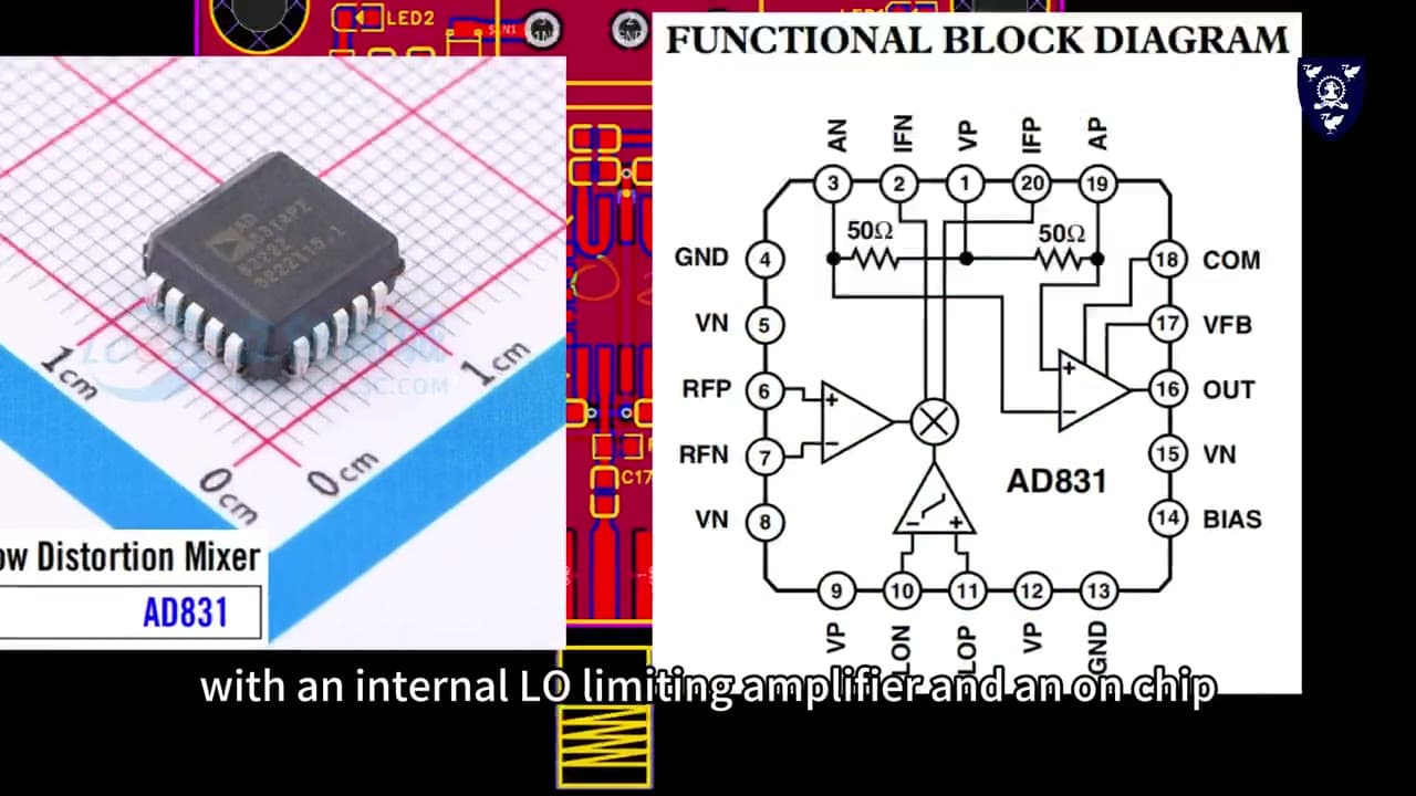 Video视频AD831 mixer demo videoAD831 混频器演示视频V1 bare board, frontV1 裸板正面V2 bare board, frontV2 裸板正面V3 bare board, frontV3 裸板正面V4 bare board, frontV4 裸板正面
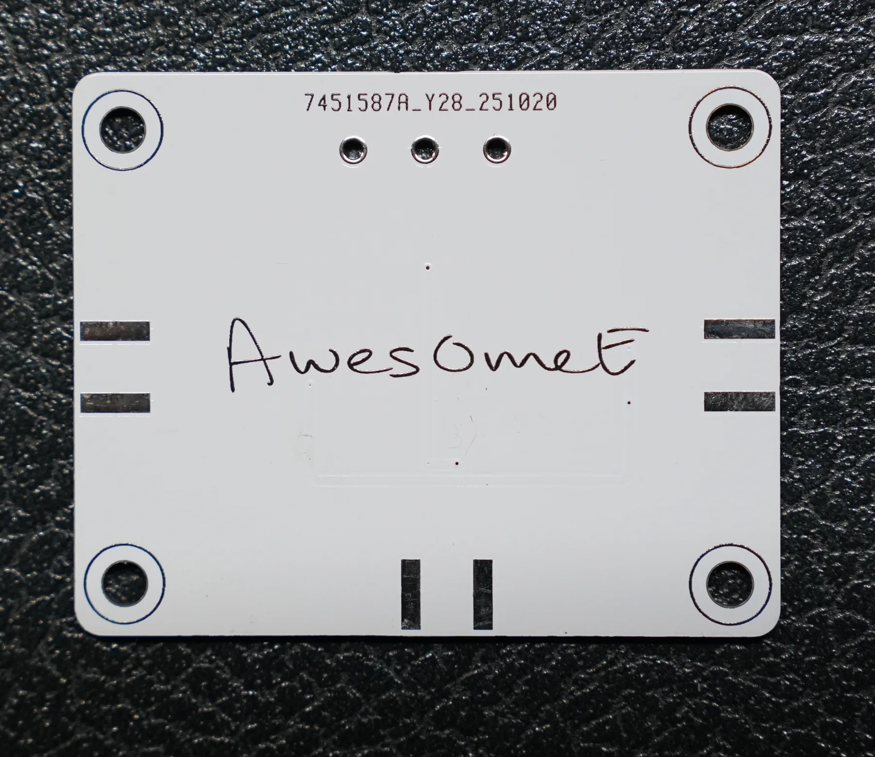 V1 bare board, backV1 裸板背面Four soldered versions, stacked叠在一起的四版成品
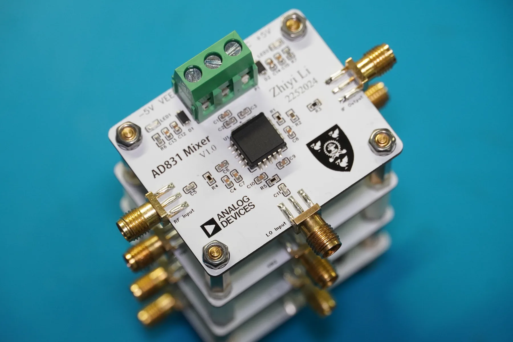 Assembled mixer board焊好的混频器板Debugging at the studio在工作室调试V4 3D renderV4 的 3D 渲染V1 3D renderV1 的 3D 渲染Final schematic最终原理图
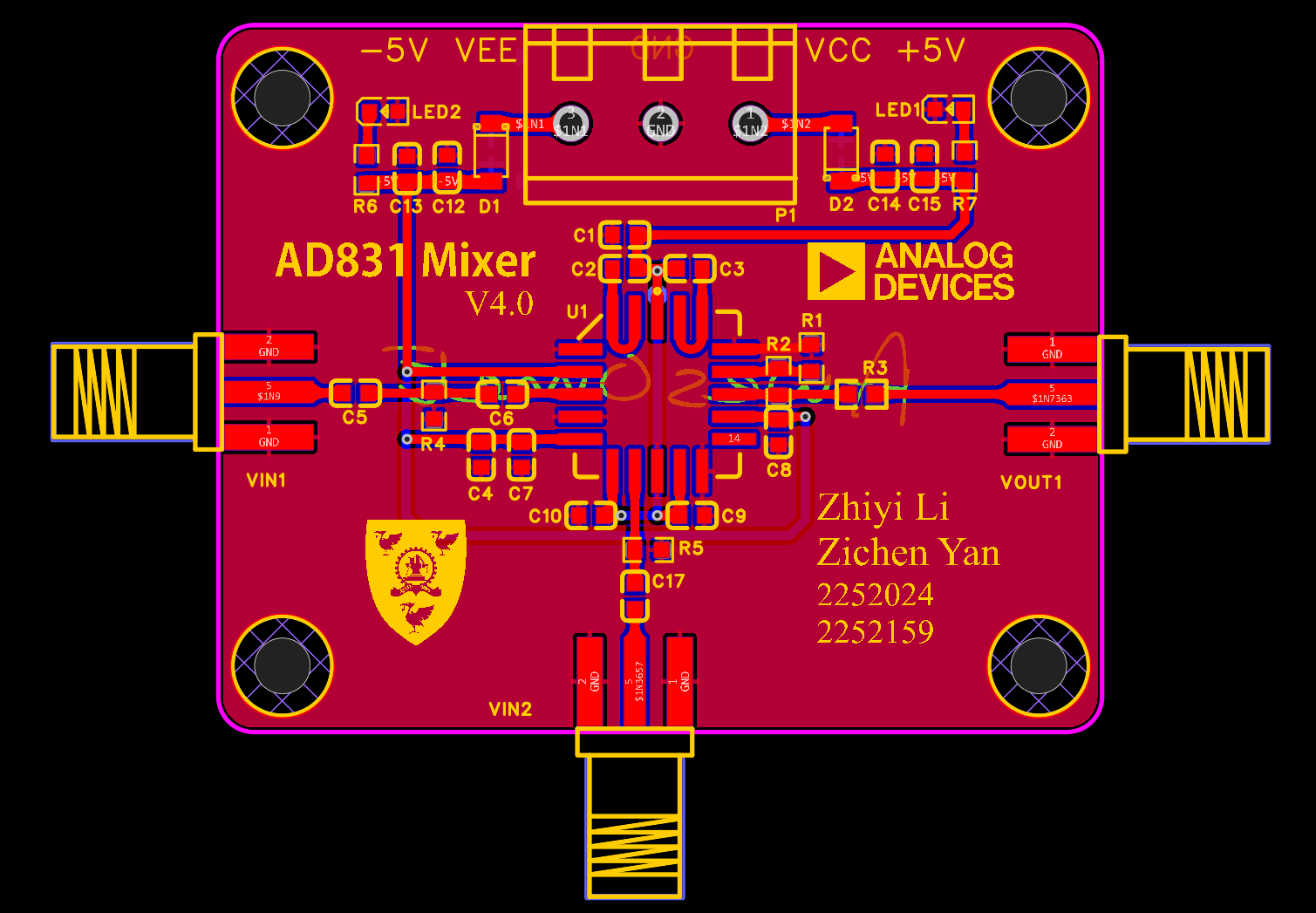 V4 PCB layoutV4 的 PCB 布局IF output on the handheld scope手持示波器上的中频输出
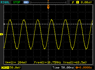 IF capture on the RIGOLRIGOL 上的中频存图IF spectrum from the RIGOL captureRIGOL 存图的中频频谱
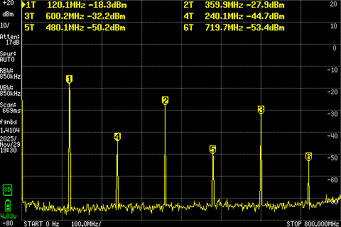 RF input spectrumRF 输入的频谱
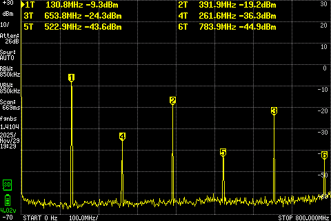 LO input spectrum本振输入的频谱